Flexible, Dual Output, 6-Phase Buck Controller Drives 12 V to 1.0 V/200 A Core Supply with 90.0% Efficiency
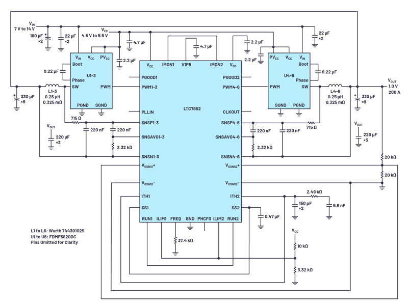
Figure 1. Schematic of a 6-phase 1.0 V/200 A LTC7852 converter with FDMF5820DC DrMos. The FSWITCH = 400 kHz.
ASICs, FPGAs, and processors in high-performance communication, servers, and computing systems require core power supplies that can produce voltages of 1.0 V (or less) directly from a 12 V or intermediate bus—with maximum load currents sometimes above 200 A. These supplies must meet stringent efficiency and performance specifications, often within a relatively small PCB footprint. The LTC7852/LTC7852-16-phase, dual output, buck controller enables high performance and flexible solutions for these supplies.
The LTC7852/LTC7852-1 is designed for high efficiency. Instead of using internal gate drivers, each phase of the LTC7852 produces a PWM output that interfaces with power blocks, DrMOS, or external gate drivers and discrete MOSFETs. DrMOS devices result in an overall smaller solution size and high efficiency by integrating the gate drivers and MOSFETs in one package. They are typically designed for 12 V input voltages. External gate drivers and MOSFETs yield good thermal performance and can operate with higher input voltages. The sub-mΩ DCR sensing architecture of the LTC7852 allows accurate current sensing with DCR values of only 0.2 mΩ. This greatly reduces conduction losses. The LTC7852-1 is designed to work specifically with DrMOS devices that provide their own current sense signals.
Each output is differentially sensed and has a range of 0.5 V to 2.0 V (the 2.0 V limitation only applies to the LTC7852) with a total regulation accuracy of ±0.5%. Because the LTC7852 and LTC7852-1 are biased from an external 5 V supply instead of the input voltage, the input voltage range of the converter is not limited by the IC. Its switching frequency range is 250 kHz to 1.25 MHz, while the 40 ns minimum on-time allows for high step-down ratios.
Phase configurations of 3+3, 4+2, and 5+1 for the two outputs can be selected with the PHCFG pin. In a 3+3 configuration, the two outputs can be paralleled for a 6-phase converter with maximum load currents of 240 A. Using one 6-phase controller instead of two 3-phase or three 2-phase controllers greatly simplifies design and layout. Up to 12-phase operation can be realized with only two controllers.
The LTC7852 is packaged in a 5 mm × 6 mm GQFN and the LTC7852-1 is packaged in a 4 mm × 5 mm QFN.
6-Phase High Efficiency Core Supply
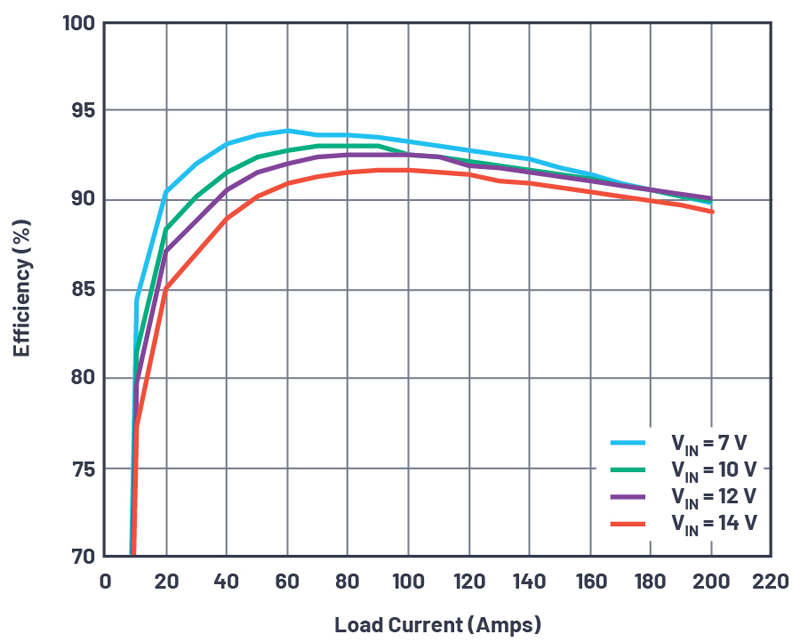
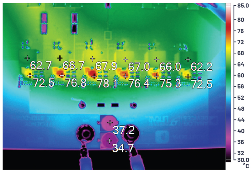
Figure 1 shows a 6-phase 1.0 V/200 A LTC7852 converter. It operates at a switching frequency of 400 kHz and with a 12 V input. The power stage of each phase consists of a 5 mm × 5 mm DrMOS and a 0.25 µH ferrite inductor with a typical DCR of 0.325 mΩ. The resulting full load efficiency is 90.0% (Figure 2). The hot spot temperature with full load, 200 LFM airflow is 78°C at room temperature (Figure 3). Due to the tight current sharing, the temperature difference between inductors is less than 6°C.
Click image to enlarge
Figure 2. Efficiency plot of the circuit of Figure 1 at VIN = 7 V, 10 V, 12 V, and 14 V
Click image to enlarge
Figure 3. Thermal image of the circuit of Figure 1 at VIN = 12 V, full load, 24°C ambient temperature, and 200 LFM airflow
Sub-mΩ DCR Sensing
The LTC7852 employs a proprietary peak current-mode sub-mΩ DCR sensing architecture to improve the signal-to-noise ratio of the current sense signal. A DCR sense filter across the inductor provides the SNSP and SNSN pins with an amplified ac signal. A second filter cascaded with the first provides a dc signal to the SNSP and SNSAVG pins. The LTC7852 amplifies the dc signal and sums it with the ac signal to reconstruct the signal. The reconstructed signal is a 5× multiple of the original. This allows clean and stable operation with DCR values as low as 0.2 mΩ.
Output Current Monitoring and Overcurrent Protection
The LTC7852’s IMON1 and IMON2 pins produce a signal proportional to the load currents of their corresponding channels and referenced to the V1P5 pin. This signal can be used by a power supply monitor or an ADC and microcontroller for load detection.
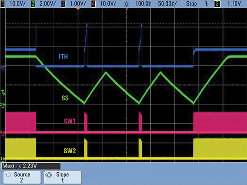
Cycle-by-cycle current limiting is a native benefit of the peak current-mode architecture. The hiccup-mode current limit provides additional protection. If an overcurrent fault is present for more than 32 cycles, the converter stops switching for a length of time programmed by the soft start capacitor. At the end of this interval, switching resumes with soft start. As shown in Figure 4, the converter switches for a relatively short period of time during the fault. This results in much lower thermal stress on the MOSFETs and inductors.
Click image to enlarge
Figure 4. Hiccup-mode overcurrent protection and recovery
Conclusion
The LTC7852/LTC7852-1 is a high performance, flexible, 6-phase, dual output buck controller intended for high efficiency and high reliability supplies using DrMOS, power blocks, or external gate drivers and MOSFETs. Its features include sub-mΩ DCR sensing (LTC7852), selectable phase configurations, a 0.5 V reference with ±0.5% total regulation accuracy, differential output sensing, a 250 kHz to 1.25 MHz switching frequency range, and hiccup-mode current limit protection.