Floating Ground Hot-Swap Architecture for Data Centres

This paper proposes a design to address the challenges of hot-swap protection for 800V data cente architectures
Figure 1: Data Center Power Distribution Architecture Evolution
The exponential growth of AI, high-performance computing (HPC), and cloud services is driving an unprecedented surge in data center power demands. Traditional 50V DC power distribution architectures, once sufficient for kilowatt-scale IT racks, are rapidly approaching physical and economic limits as AI workloads push rack densities from 10kW–30kW to over 100kW, and eventually toward 1MW. Data center power architectures are transitioning from traditional power shelves to power sidecars, where power is delivered to IT racks on an 800V or ±400V HVDC bus.
In an HVDC power architecture (Figure 1-1), the three-phase 480V AC power from the utility grid is converted into an 800V or ±400V DC bus using high-efficiency rectifiers. Through a hot-swap circuit, the power from the HVDC bus is fed into an intermediate bus converter (IBC) module, which converts the 800V or ±400V DC to intermediate voltages (for example, 48V, 12V, or 6V) for server racks. Finally, the power is stepped down to the GPU supply voltages of less than 1V using multiphase DC-DC power converters. The HVDC domain introduces new challenges for system protection and monitoring, particularly during hot-swap events. To address these challenges, a floating ground hot-swap architecture is proposed.
Floating Ground Hot-Swap Architecture
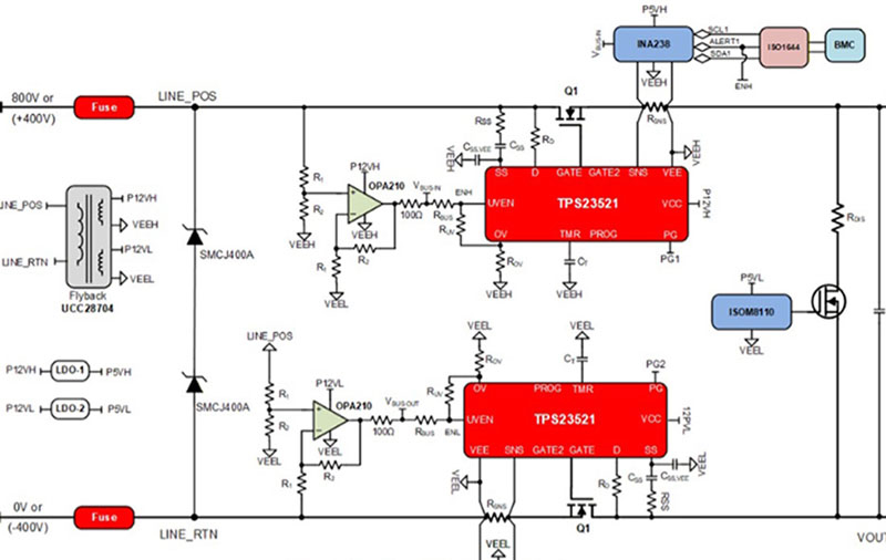
A high-voltage hot-swap architecture based on the floating ground concept uses TI’s TPS23521 low-voltage, low-side, hot-swap controller to provide standard hot-swap functions such as hot-plug, inrush current management, undervoltage, overvoltage, overcurrent, and short-circuit protections.
TPS23521 uses VEE as a reference and drives the GATE of the hot-swap FET. Unlike in a standard hot-swap configuration, the controller reference is left floating and connected to the load terminal instead of to the system ground. By powering between the VCC and VEE pins through an isolated bias power supply, the system emulates a scalable, floating ground hot-swap architecture making the TPS23521 appropriate for ±400V or 800V rails.
The capacitor (CSS), connected between the SS pin and the FET drain through a 1kΩ resistor, determines the slew rate of the GATE voltage during start-up. The CSS is internally connected to the GATE pin, functioning as a gate-to-drain capacitor for Q1. When VCC is applied, the TPS23521 device begins GATE charging and turns on Q1. Once the gate-to-source voltage crosses the VTH, the entire GATE current discharges the CSS capacitor, thereby linearly discharging the drain-to-source (VDS) voltage of Q1. The FET Q1 operates in the Miller plateau region and acts as a source follower, where VOUT follows the GATE with a slew rate determined by the CSS capacitor. When the VDS of Q1 reaches zero, the GATE to VEE voltage increases further to VCC to VEE, enabling Q1 to operate in full conduction mode. The low-side current sensing keeps the overcurrent and short-circuit protections intact during start-up and steady-state conditions.
System Design Considerations
Leveraging the floating ground hot-swap architecture discussed in the previous section, a complete hot-swap solution is built by using TI products; UCC28704 flyback controller to generate the bias power supply; OPA210 operational amplifier in a differential configuration to scale down from the 800V input power supply voltage and interface with the UVEN and OV pins of the TPS23521 device; INA238 for precise current, voltage, and power monitoring through I2C to enable digital telemetry for intelligent rack management; ISOM8110: Opto-emulator to provide an isolation barrier.
Click image to enlarge
Figure 2: Block Diagram of the Floating Ground Hot-Swap Solution on High-Side and Low-Side Power Paths
Figure 2 shows the floating ground hot-swap architecture allows a truly scalable solution, whether of the power level or supply rail voltage ±400V / 800V, making the architecture compatible for installations with either two wires or three wires.
Design Guidelines and Component Selection
Click image to enlarge
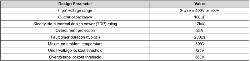
Table 1: Typical System Specifications
A current sense resistance of 1mΩ, 3W (WSL39211L000FEA) is used in this design.
Capacitors, CSS and CSS,VEE : Compute the minimum inrush current where the timer runs during start-up using -
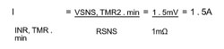
To avoid running the timer during inrush, the inrush current must be sufficiently lower than 1.5A. Target 200mA of inrush current for a better FET SOA margin during start-up. Compute the target CSS using -
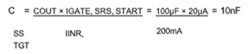
Two multilayer ceramic capacitors (GRM32E5C2J223FWA3L), 0.022µF, 630VDC, and C0G are used in series for CSS. TI recommends adding a capacitor CSS,VEE that is three times larger than CSS between the SS pin and VEE to improve transient immunity during soft start.
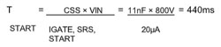
Finally, the start-up time can be computed using -
Selection of VDS switch-over threshold: The threshold voltage at which the TPS23521 device switches from the lower current threshold (3mV/RSNS) to the higher current threshold (25mV/RSNS) can be selected through a resistor RD. A higher VDS threshold provides better transient immunity but exposes the FET to increased SOA stress. Start with a VDS switch-over voltage of 100V and calculate RD using -
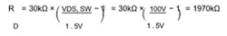
Three resistors (TNPV1206680KBEEN) 680KΩ and 700V are used in series. The effective switch-over voltage is obtained as 103.5V.
Fault timer selection: The timer determines how long the hot-swap can allow overload before timing out and can be programmed using CT. To set 200µs -
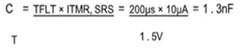
A ceramic capacitor (CC0603JRX7R8BB152), 1.5nF is used.
The OPA210 device is used as a differential amplifier to scale down (gain of R2/R1) and monitor the input bus voltage. Select resistors R1 and R2 to set gain of 1/10 -
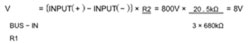
The scaled bus voltage VBUS-IN is used to set the undervoltage and overvoltage threshold on the input bus by following the standard process in the TPS23521 datasheet.
The silicon carbide (SiC) combo JFET (UG3SC120009K4S), 1200V, and 8.8mΩ is used in this design. The FET SOA must be analyzed for stressful events, such as start-up, start-up into short, and overcurrent events.
During start-up, with an inrush current of 100mA, the system takes approximately 440ms to charge a 100μF output capacitor from 0V to 800V. The UG3SC120009K4S FET can support > 300mA at 70°C with a drain-to-source voltage of 800V, thus providing an SOA margin of > 50%
During a start into short, the gate ramps up very slowly due to a large capacitance at the gate through the SS pin. To evaluate the FET stress, the current pulse must be approximated as a rectangular pulse. In this design, the FET stress is approximated with a 500µs (the equivalent rectangular pulse of the current waveform), 1.5A, and 880V pulse. The UG3SC120009K4S FET can handle a current pulse of 2.2A for 500µs at 880V and a junction temperature of 100°C, thus giving an SOA margin of 50%.
During an overload event, the TPS23521 device operates in current limiting mode, which is a risk for the hot-swap FET. To overcome that risk, the INA238 device is configured with an overcurrent alert at 22A, and the alert output of the INA238 device is used to disable the TPS23521 device at the UVEN pin. This function emulates a circuit breaker event without causing any stress on the FET.
The TPS23521 device generates power good (PG) signals with reference to the grounds VEEH and VEEL of the TPS23521 device. These signals are passed through digital isolators and then combined to control the downstream load, which avoids load during start- up, thereby placing very low SOA stress on the hot-swap FETs.
To meet the safety requirements of the IEC 62368-1 standard, the hot-swap solution has incorporated a circuit to discharge the output capacitance in <2 seconds. When the hot-swap FET is turned OFF, or the input is disconnected, the discharge resistor (RDIS) is engaged to discharge COUT. A 2kΩ, 10W resistor (AC10AT0002001JAB00) is selected to discharge 100µF in 1.5 seconds.
The transient protection component, TVS diode, can be selected by following the guidelines outlined in reference 3. Two SMCJ400A diodes connected in series are placed at the input side.
Test Results
Click image to enlarge
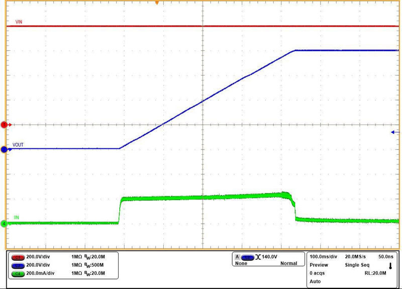
Figure 3: Start Up at 800V With 100µF Capacitance
Click image to enlarge
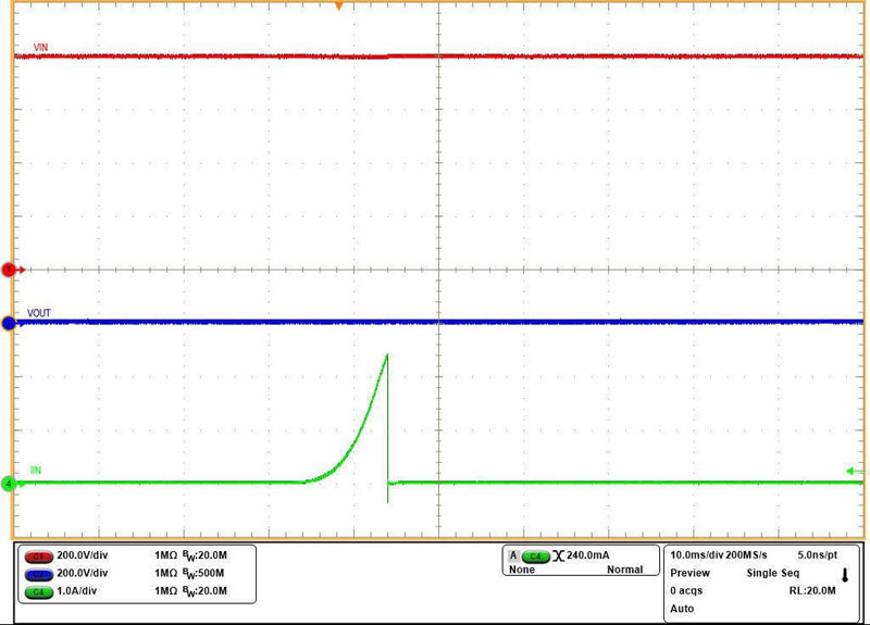
Figure 4: Start Up Into Short at 800V VIN
Click image to enlarge
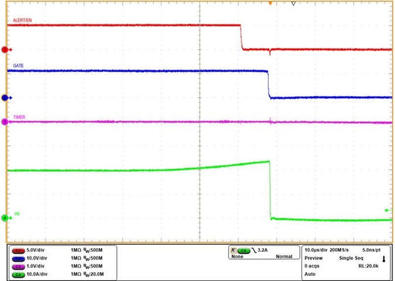
Figure 5: Circuit Response During Gradual Overcurrent
Figure 3 shows the inrush behavior during start-up while charging a 100μF capacitance to 800V. Figure 4 illustrates the start-up behavior of the circuit with a short-circuit at the output terminals. As demonstrated, the current peaks to 3A (lower current limit level), where the TPS23521 device detects and terminates the fault path. In case of a gradual overcurrent fault, the INA238 device alerts at 22A and pulls down the EN pin of the TPS23521 device, thereby disabling the hot-swap FET in 10µs, as shown in Figure 5.
Click image to enlarge
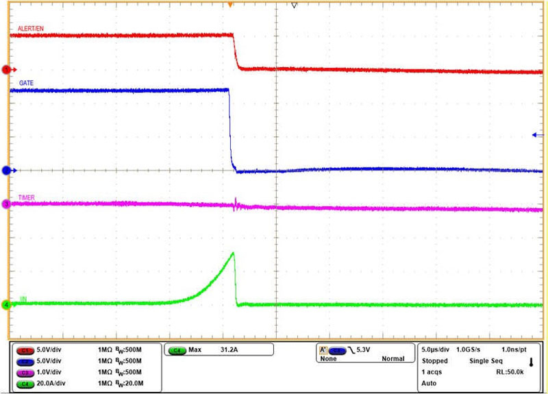
Figure 6: Circuit Response During an Output Short Circuit
Figure 6 shows the circuit behavior during an output short-circuit fault in the steady state. The INA238 and TPS23521 devices both detect the fast-rising short-circuit current and disable the FETs in a few µs.


