Silicon Carbide Semiconductors: Gaining Widespread Adoption

Higher efficiency and power density are accelerating SiC adoption
Silicon carbide (SiC) semiconductors improve energy efficiency and switching performance in electric vehicles. Until now, the cost-benefit ratio has been particularly favorable for high-performance premium models. But the balance is shifting. Improved power density and robustness are making SiC MOSFETs increasingly attractive for the broader market. The new generations of chips from Bosch show that development is gaining momentum.
In a battery-electric vehicle, the power electronics control every flow of energy – from the power supply to the drive, and from the grid to the battery. The key components are the traction inverter, which converts the direct current from the high-voltage battery into alternating current for the electric motor; the DC/DC converter, which matches different voltage levels; and the on-board charger (OBC). In all three applications, high resistances and switching losses have a direct impact at system level: reduced range, longer charging times, or unnecessarily large and heavy components.
Why SiC is superior
Silicon carbide excels precisely in these high-voltage electronic components, which must deliver reliable performance under demanding conditions such as high voltages, frequencies, or temperatures. As a so-called wide-bandgap material, SiC has significantly higher critical electric field strength, improved thermal conductivity, and more efficient electrical switching behavior than conventional silicon. A traction inverter with SiC MOSFETs (metal-oxide-semiconductor field-effect transistors), for example, enables a longer range or, depending on the vehicle segment, a smaller battery while maintaining the same performance.
Bosch is developing several generations simultaneously
Bosch does not develop SiC generations sequentially, but rather in parallel: Several technology paths mature simultaneously. In this process, interdisciplinary teams comprising development, laboratory, manufacturing, and quality management work closely together, ensuring that each generation can transition to production with a high level of industrial reliability. “At the same time, our solutions are precisely coordinated with one another,” explains Anne Bedacht, head of product management for power semiconductors at Bosch. “We always keep the next development step in mind from the very beginning. This allows us to anticipate that our chips will continuously improve their performance.”
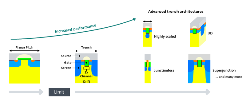
The foundation is Bosch’s proprietary vertical trench architecture, in which the gate – the transistor’s control electrode – is not arranged in a planar configuration on the chip surface, but instead extends vertically into the SiC material. Both sides of the trench are used as current channels, which increases channel density and reduces resistance. “The next evolutionary steps for SiC would be impossible to implement without trench technology,” Anne Bedacht points out. “It enables smaller chip areas with higher power density and robustness. This leads to cost advantages at system level.” The third generation of Bosch’s SiC MOSFETs, which made its debut at this year’s PCIM in Nuremberg, Germany, marks the next step of this development journey.
Click image to enlarge
Figure 1: Trench technology forms the foundation for all future technology paths in Bosch’s upcoming SiC MOSFET generations
The improvements of Gen 3
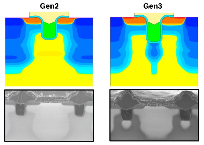
With its third generation of SiC MOSFETs, Bosch is further refining the trench architecture. At its core there is an additional shielding implantation within the trench itself, which completely shields the gate oxide from electric fields during reverse operation. “This again significantly increases the long-term reliability of the gate,” says Anne Bedacht. “The gate has historically been a critical component in SiC transistors.”
Click image to enlarge
Figure 2: Cross-section comparing Gen 2 and Gen 3 cell architectures – trench structure (green), shield implantation beneath the trench (blue), and JFET region (yellow)
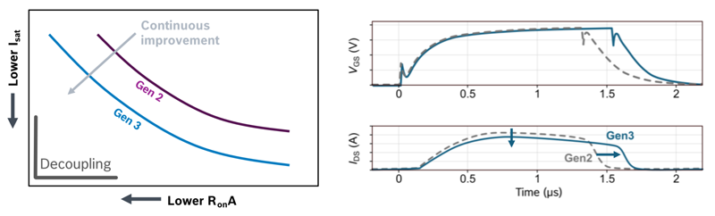
The newly designed two-zone JFET (junction field-effect transistor) region below the trench ensures more uniform current distribution and a faster response time of the gate driver in the event of a fault. Optimized distribution of parasitic capacities, i.e. unavoidable electrical couplings between the device’s internal electrodes, reduces switching losses in typical traction inverter operation by about 10 percent and enables faster switching operations. To achieve this, part of the gate-drain capacitance (CGD) is shifted to the gate-source capacitance (CGS), thereby reducing the gate-drain charge (QGD). This reduces the Miller factor and thus the risk of parasitic turn-on. A comparatively high threshold voltage (Vth), supported by a thicker gate oxide in the trench, provides additional protection. Overall, short-circuit withstand capability increases by about 10 percent compared to the previous generation. This is also reflected in the improved trade-off between on-resistance (RonA) and saturation current (Isat), as well as in lower current density and an extended time window for shutdown in the event of a short circuit (see figure 3).
Click image to enlarge
Figure 3: Compared to Gen 2, Gen 3 offers an improved trade-off between on-resistance (RonA) and saturation current (Isat). Simultaneously, the time window for detection and shutdown is extended in the event of a short circuit
In addition to the modified trench architecture, Bosch reduced the chip thickness by 40 percent, which improves heat dissipation. “Compared to Gen 2, Gen 3 delivers a higher overall power density and a 20 percent lower on-resistance (RonA), thereby reducing the required chip area while maintaining the same power output,” Anne Bedacht reports. The additional shield implantation was achieved by reusing the existing trench hard mask, i.e. without significantly increasing manufacturing complexity. Generation 3 is expected to be available to OEMs starting in 2027, manufactured on 200 mm wafers, to which Bosch has been gradually transitioning since 2024.
Outlook: Gen 4 und 5
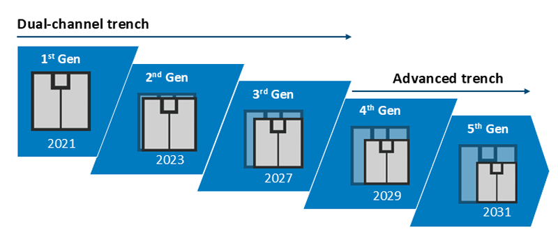
In line with the parallel development approach, work on the next generations is already underway. Generation 4, which Bosch expects in 2029, will deliver a radical leap in scaling thanks to an extremely narrow pitch design: The cell pitch (i.e. the distance between adjacent transistor cells on the chip) will decrease from about 3 to less than 2 micrometers. This type of vertical integration is achievable exclusively with trench technology, as planar architectures are generally limited due to their surface-bound gate and channel geometries. The result is even smaller chips with the same performance, combined with immediate cost advantages for module and inverter designs. Nevertheless, Gen 4 will not require a fundamentally new component concept but can still be integrated into proven MOSFET system architectures.
With Generation 5, which Bosch plans to launch in 2031, a new concept will be introduced to SiC chips for the first time: superjunction technology. By alternating p- and n-doped structures in the drift zone, the technology falls below the previous physical minimum for on-resistance, the so-called unipolar material limit, of SiC. This creates a new performance class with further reduced resistance and stable high-voltage performance. “With this technology, an increase in manufacturing complexity is unavoidable. However, the improvements are so significant that the investment is worthwhile. Furthermore, superjunction will enable additional design improvements that are currently not yet cost-effective. So things will remain exciting for future generations as well,” Anne Bedacht reveals. Current development efforts focus, among other things, on suitable manufacturing processes as well as the control of self-excited oscillations, which can occur at very high switching speeds and lead to voltage spikes, switching losses, and electromagnetic interference (EMI).
Click image to enlarge
Figure 4: Bosch's SiC MOSFET generations – smaller chip sizes with increased power density
Stable production conditions
At Bosch, the performance leaps achieved by each generation go hand in hand with an expansion of manufacturing capacity. Starting in 2027, all new SiC generations will be designed exclusively for 200 mm wafers, which offer twice as much surface area as the previous 150 mm wafers. Production will take place at the Reutlingen site in Germany, where series production has been underway since 2021; in addition, production is scheduled to begin in Roseville, California, in 2026.
The 200 mm technology not only increases the number of chips per wafer but also improves manufacturing precision and chip uniformity. “The more sophisticated our semiconductors become, the more important these stable production processes are. That’s why we transfer technologies from the research cleanroom to actual production conditions as early as possible, which allows us to deliver sooner,” Anne Bedacht explains.
A shift in cost calculation
Each generation of Bosch’s SiC MOSFETs reduces chip size while maintaining the same performance. Robustness and efficiency increase, and the economies of scale from 200 mm manufacturing take effect. This all adds up to a shift in the cost-benefit analysis: SiC is becoming attractive not only for high-performance vehicles with 800 V architecture, but increasingly also for 400 V platforms in the mid-size and compact classes. Greater range, efficiency, and robustness will no longer be the exclusive privilege of the upper vehicle segments: The technological journey of SiC across the spectrum of electromobility is gaining momentum.