How Infineon shapes power for growth through MOSFET innovation
Our world has experienced dramatic change over the past 50 years. New economic, social and technological trends have emerged significantly impacting our way of life in different ways. Regardless of the way and degree to which the world has been changing, one thing remains: technology plays a crucial role in it.
Whether we think about electro mobility, internet of things, artificial intelligence, connectivity or 5G, all are heavily technology-driven innovations of today and tomorrow. These new application areas not only have profound implications for our lives, but also for underlying design requirements. Design engineers face new challenges in their jobs every day: adapting new power architectures and increased bus voltages, needing more power in small form factors, demanding higher levels of power density and energy efficiency. Looking at the value chain behind the solutions that respond to these challenges, it all comes down to the tiniest detail: the microchip. System performance (including reliability aspects) hinges on the selection of the right power switches.
At the forefront of key power semiconductor innovations
With more than 40 years of experience in power MOSFET innovation, Infineon has led the way in solving the challenges design engineers face on a daily basis while helping engineers achieve their targets. Although these targets may have changed over the years, the innovative spirit behind Infineon’s product offering has persisted – from device design, technology-, package- and product development through manufacturing.
Looking at the evolution of MOSFETs in the industry, numerous advancements in MOSFET technology have enabled the applications and trends that have become an indispensable part of our lives. Consider the introduction of the first hexagonal topology MOSFETs in 1979 or the new generation of MOSFET technology launched in 1995 which was based on an advanced four-mask process utilizing innovative self-alignment features to improve manufacturing precision and increase yields. That process enabled MOSFETs to be manufactured with a low cycle time (compared with requirements for the six-step process) and allowed junction depths up to 40 percent smaller than conventional processes thereby greatly reducing the transistor junction resistance while increasing ruggedness.
Shortly after these technological developments, the world’s first FETKY product was introduced integrating the MOSFET and a Schottky diode into a single package reducing form factor and losses in DC-DC applications. Later, in 1999, leveraging manufacturing expertise, a stripe planar technology with a fully self-aligned manufacturing process that featured high density planar structure providing extremely low on-resistance, excellent high-frequency operation, industry-best ruggedness and excellent manufacturing cycle time was introduced. The same year, a family of MOSFETs with the industry's highest cell density and lowest RDS(on) trench MOSFETs was also introduced. That technology focused on the latest products for handsets, laptop computers and a variety of other portable electronic devices, paving the way for ever-better performing products in the market.
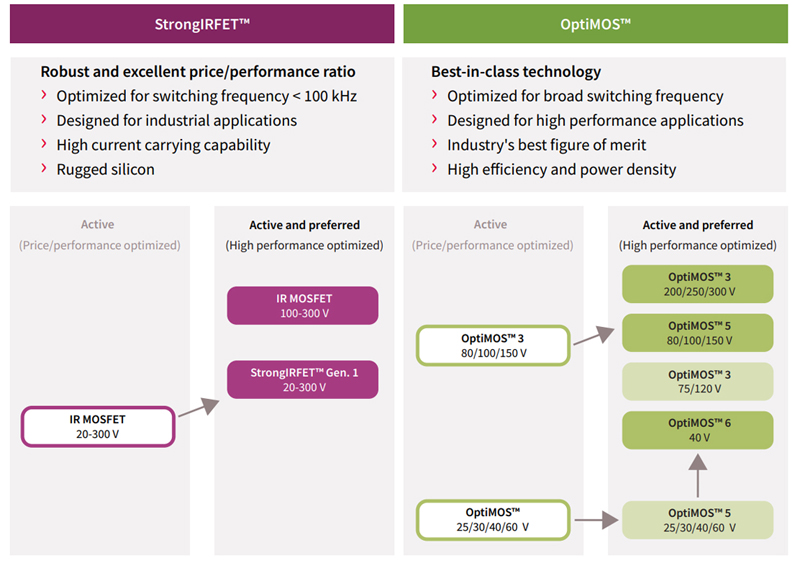
In 2000, the first family of OptiMOS™ MOSFET technology featuring ultra-low switching losses for high efficiency to help designers increase power density was launched. The OptiMOS™ family has evolved throughout the years and is now in its sixth generation. OptiMOS™ products offer an impressive reduction in RDS(on) combined with superior switching performance. The OptiMOS™ family is optimized for a variety of applications and circuits, such as synchronous rectification in switched mode power supplies (SMPS) in servers, desktop PCs, wireless chargers, quick chargers, and OR-ing circuits. Additionally, in 2012, the StrongIRFET™ family of MOSFETs optimized for low RDS(on) and high current capability – making them the ideal choice for low frequency applications requiring performance and ruggedness – was also introduced to the market.
Packaging innovation has also been at the heart of Infineon MOSFET development. In 1993, the SOT-223 was introduced as the first surface mount power MOSFET in the industry. In 2002, the DirectFETTM power package was introduced as a proprietary surface mount package featuring a new interconnection methodology with radical gains in both conduction and thermal efficiencies. In 2013, the widely utilized TO-Leadless package that allows for high current capability in a reduced footprint compared to a traditional D2PAK was introduced. Most recently, Infineon has launched a family of OptiMOS™ power MOSFET devices in a PQFN 3.3 x 3.3 Source-Down package with a flipped die inside to allow for improved thermal performance and reduced RDS(on).
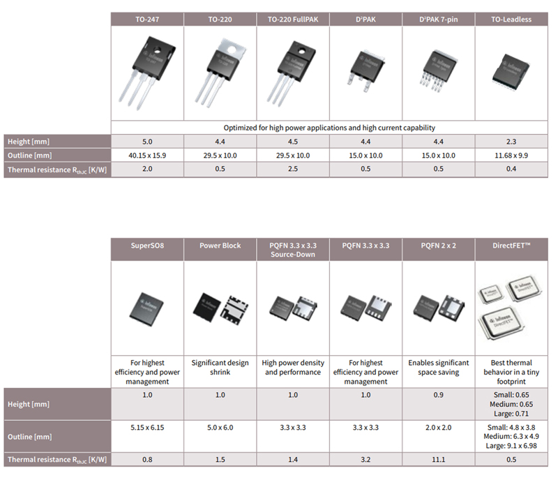
Click image to enlarge
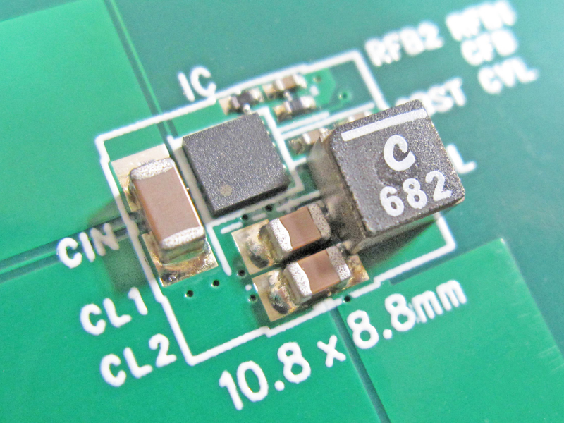
Figure 2: Space-saving and high performance packages in the StrongIRFET™ and OptiMOS™ product families
Let’s take a closer look at what benefits packaging innovations can bring to an application.
Innovating on chip-level for system performance
The chosen application example is artificial intelligence. Power management – more specifically, the power density of the power converters fueling the processors and ASICs in a system – is one of the biggest challenges designers face in enabling artificial intelligence and keeping up with the calculation and storage needs in the cloud.
With the introduction of 48 V bus voltage, some additional power conversion is introduced into the power chain. This conversion has to be done close to the payload to avoid transmission losses and benefit from the higher bus voltage. With Infineon’s Hybrid Switched Capacitor (HSC) resonant DC-DC converter, innovation is at the system-level by utilizing Infineon’s newest Source-Down OptiMOS™ power MOSFETs. This new topology shows great potential to offer higher power density and efficiency levels than the current solution. Combined with Infineon’s new Source-Down product portfolio, this solution can be optimized from the ground up, component-level innovation with the system in mind.
Let’s take a look at how this is done.
Addressing power density challenges requires innovation at the component level with advancements in resonant topologies. With the introduction of Infineon’s Source-Down package technology, the IQE006NE2LM5 further enhances electrical and thermal performance, enabling the power density needed in modern datacenter applications. The main benefits of the innovative package include:
- 30 percent lower RDS(on), decreasing I²R losses
- Lower package-related parasitics, reducing the FOM and leading to lower switching losses
- Lower Rthjc, optimizing the distribution of the generated heat from the package
- Thermal pad located on the source pin, enabling optimized layouts where the large GND area can be utilized as a heatsink
To compare the performance benefits, two versions of an 8:1 hybrid switched-capacitor (HSC) converter board were examined. One is based on a standard Drain-Down device (BSZ011NE2LS5I) and the other on the new Source-Down device (IQE006NE2LM5). Figure 2 shows the thermal performance of the devices. With the traditional package a hot-spot can be observed (Figure 3a) that is eliminated with the use of the new Source-Down package (Figure 3b). The surface temperature of the MOSFET is significantly improved, showing a 9°C difference compared to theDrain-Down device. Figure 4 illustrates the efficiency comparison (including auxiliary losses). The higher efficiency of the system featuring the new Source-Down device leads to a significant increase in power density as well.
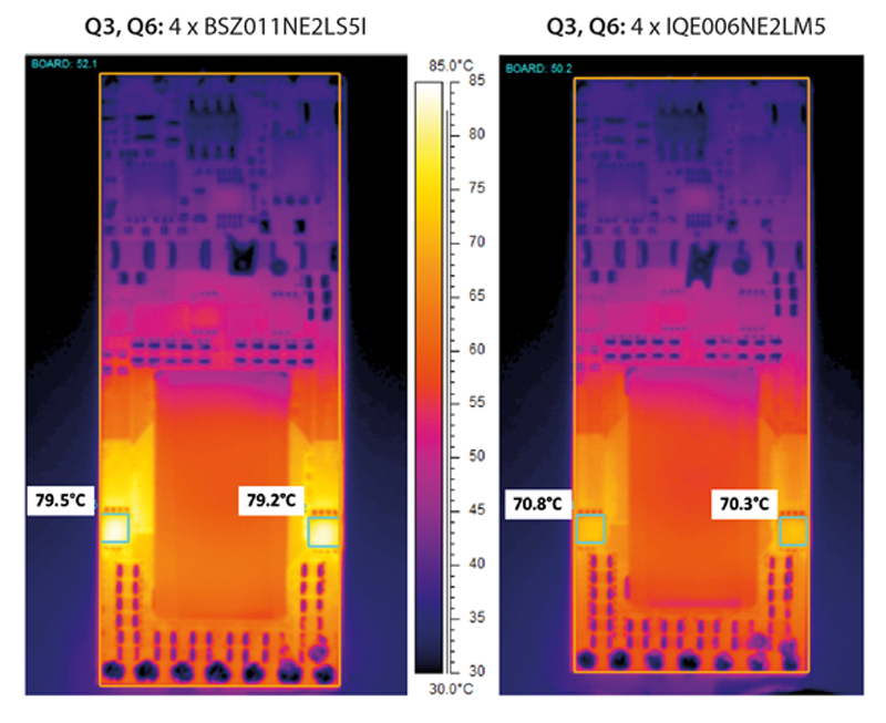
Click image to enlarge
Figure 3: The thermal behavior of the HSC at 450 W from 48 V input at 
a) with BSZ011NE2LS5I, b) with IQE006NE2LM5
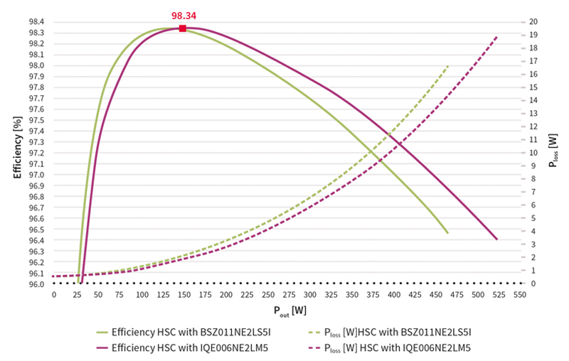
Click image to enlarge
Figure 4: The HSC converter efficiency from 48 V to 6 V, including auxiliary losses, with the BSZ011NE2LS5I and with the IQE006NE2LM5 at 
![]()
The current megatrends shaping everyday life pose tough challenges for design engineers and semiconductor manufacturers. For more than 40 years, Infineon power MOSFET innovation has proven that optimization at the component level brings significant system-level performance advantages and contributes to an easier, safer and greener future.

Scan the QR-code for the latest information on Infineon’s innovative low-voltage MOSFET solutions