Combines enhanced semiconductor chip characteristics and improved packaging structure
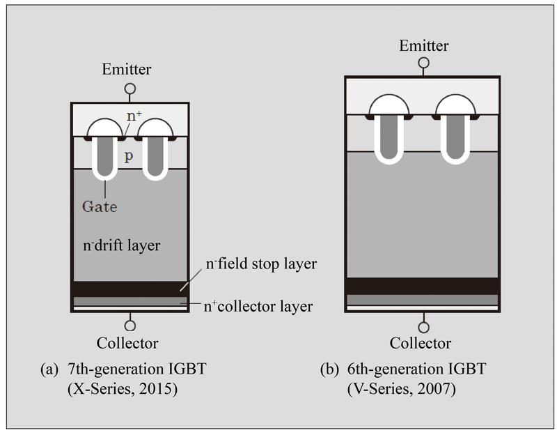
Figure 1: IGBT cross sectional structure
Fuji Electric 7th Generation IGBT Technology Powers Today’s High Efficiency Energy Conversion Systems
Today’s Power Electronic market is driving development of compact, low-loss, and, high-reliability IGBT modules to optimize power conversion systems. In response, Fuji Electric has developed our 7th generation X-Series IGBT technology combining enhanced semiconductor chip characteristics and improved packaging structure. Our unique design concept increases the IGBT performance and allows continuous 175ᵒC Tvj(op)operation. In particular, the Fuji Electric X-Series Dual XT module is the first IGBT module to achieve 800A-1200V rating in a 62 mm X 150 mm 2:1 package.
Global energy consumption is steadily increasing with a growing population and higher economic prosperity across our global community. Considering the negative environmental effect of addressing the demand with conventional fossil-fuel based energy systems, many countries are meeting the ever-increasing demand for energy with renewable energy technologies, i.e. wind and solar. Furthermore, demands for mobility electrification are driving development of robust and high-efficiency power electronic modules to replace ICE powered vehicles, i.e. automobiles, trucks, and, buses with electric vehicles (xEV).
To support the development of the high-efficiency power conversion systems needed to address these applications, Fuji Electric developed an enhanced insulated gate bipolar transistor (IGBT) technology. The new Fuji Electric 7th generation technology combines innovations in the intrinsic characteristics of our trench gate IGBT structure and free-wheeling diode (FWD) to improve and optimize performance and increase efficiency.
Fundamentally the Fuji Electric 7th generation IGBT technology simultaneously and significantly reduces IGBT and FWD losses, power dissipation, and, accomplishes chip miniaturization. Through the following enhancements, internally and externally, the development addresses and successfully overcomes the various operational areas that tend to be problematic at high-temperature operation thus enabling the 7th generation IGBT to support continuous 175ᵒC Tvj(op).
In particular the improvements in the collector-emitter saturation voltage in our Dual XT 2:1 module was achieved through optimizing the thickness of the IGBT drift layer and ensuring any voltage oscillation and voltage withstand performance degradation at device turn-off associated with thinner drift layer is suppressed through a concurrent optimization of the device field stop (FS) layer.
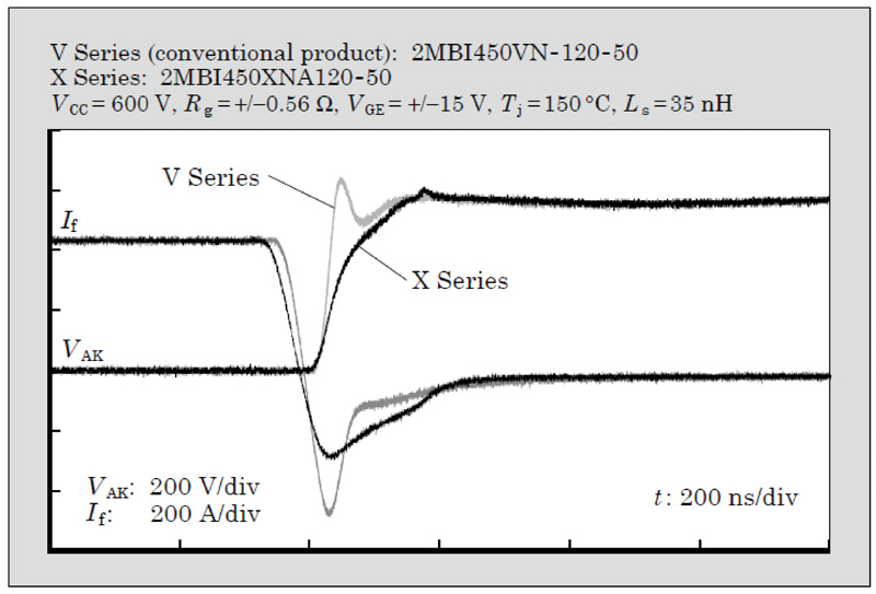
In a similar optimization, the enhancements to the FWD anode-cathode forward voltage characteristics was accomplished by reducing the FWD drift layer thickness. Additionally, through the optimization of local life-time control, the 7th generation FWD exhibits soft reverse recovery behavior during turn-off and thereby avoids potential over-voltage due to stray-inductance and high diode current di/dt. The total FWD reverse recovery energy was significantly lessened by reducing the turn-off reverse recovery and tail current. By optimizing the reverse surface of the 7th generation FWD we prevent the depletion layer from reaching the reverse surface side to minimize voltage oscillation and reverse recovery surge voltage.
Figure 1 displays the basic IGBT cross-sectional structure between Fuji Electric 6th & 7th generation IGBT technology which by comparison utilize a similar front surface trench gate structure and field stop layer back-side. The 7th generation enhancements are primarily drift and field stop layer thickness reduction and optimization of trench gate structure. Fundamentally these refinements in the front surface enable the suppression of p-channel hole pull-out during device conduction and simultaneously increase the injection-enhanced (IE) effect by increasing the carrier concentration on the IGBT front surface. These refinements significantly improve the trade-off between on-state voltage and turn-off loss of the IGBT.The enhancements made in the IGBT and FWD characteristics result in a power dissipation improvement in the 7th generation IGBT; in particular the 7th generation Dual XT 2:1 module achieves an approximate 12% reduction in power dissipation at a 1 kHz carrier frequency when compared to similar conventional IGBT modules.
The trade-off characteristics depicted in following figures differentiate the various IGBT trade-off characteristics: Figure 2 compares the 6th and 7th generation on-state voltage (VCE) and turn-off energy and the 0.4V reduction in on-state voltage, VCE(sat) and a 7% reduction in device turn-off energy.
Click image to enlarge
Figure 2: Trade-off characteristic (IGBT)
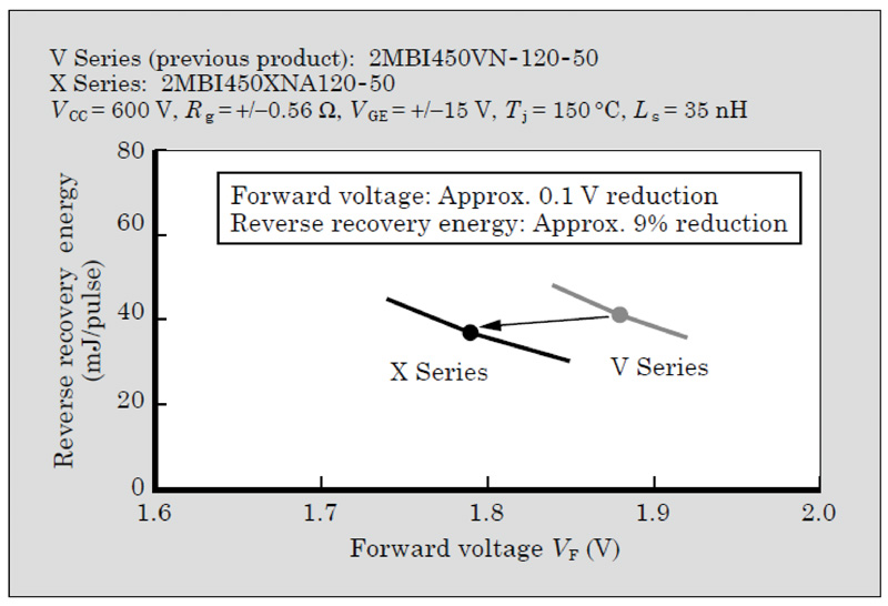
Figure 3 similarly depicts the FWD characteristic improvements of the 7th generation with an approximately 0.1V forward voltage (VF) reduction and 9% reduction in reverse recovery energy.
Click image to enlarge
Figure 3: Trade-off characteristic (FWD)
In addition, the ‘softer’ reverse recovery behavior achieved with 7th
generation FWD is evidenced by the reverse recovery waveforms depicted in Figure 4.
Click image to enlarge
Figure 4: Reverse recovery waveforms
A key feature of Fuji Electric 7th generation IGBT modules is our new packaging technology. Basically, the miniaturization of IGBT modules necessitate reducing the size of the IGBT and FWD which results in a higher device power density. Unless properly managed, the increased power density will result in higher chip temperature and ultimately reduced IGBT reliability. In order to solve the issue Fuji Electric developed a high-heat dissipating package technology.
The new 7th generation packaging technology improves both package exothermicity and overall thermal conduction to suppresses chip temperature rise, and the improvements enable continuous 175ᵒC Tvj(op) operation, and, maintains our 7th generations IGBT’s high-reliability performance capability.
To start, the internal insulating substrate represents the largest portion of the thermal resistive materials within the IGBT and though an obvious target to improve exothermicity there are inherent challenges to overcome when making changes to the substrate particularly with AlN.
To overcome these challenges Fuji Electric developed a new thin type AlN substrate with enhanced strength achieved by optimizing the ceramic sintering process and also effectively distributed the thermal stress with a highly innovative substrate circuit pattern to insure dielectric strength and resistance to cracking was maintained. The isolation properties were also improved by revising the creepage distances.
The result is the 7th generation Dual XT 2:1 premium module using a newly developed highly thermally conductive AlN insulating substrate which achieves a 45% reduction in thermal resistance compared to the widely used Al2O3 insulating substrate.
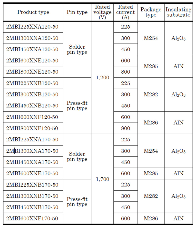
An additional consideration is internal heat generation from the internal device wire-bond connections. Conventional wire-bonds are aluminum and have a high specific resistance and hence a low thermal conductivity. The 7th generation wire bonds are copper which has a lower specific resistance and hence a higher thermal conductivity. (Table 1)
Click image to enlarge
Table 1: X Series Dual XT product line-up
The use of copper bond wires and the optimization of the circuit pattern on the AlN insulating substrate to ‘unpack’ the bond wire concentration between the terminals and insulating substrate results in a significant improvement in lowering the internal temperature rise and coupled with the external changes in the shape and thickness of the IGBT copper main terminals has significantly reduced overall heat generation.
Another key development realized with the 7th generation technology and the Dual XT 2:1 IGBT module in particular is the expansion of the continuous operating junction temperature Tvj(op) from 150ᵒC to 175ᵒC.
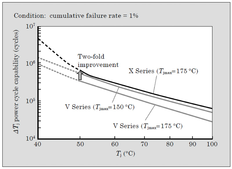
ΔTvj power cycling capability is a key figure of merit for today’s IGBT modules and is directly impacted by a Tvj(max) operational excursions exceeding 150ᵒC. Previously sustained Tvj(max) operation above 150ᵒC would dramatically degrade the IGBT modules ΔTvj power cycling capability.
Figure 5depicts the relationship between operating temperature and ΔTvj power cycling capability, in cycles; the graph shows a comparison of Fuji Electric 6th and 7th generation and two-fold improvement in power cycling capability at 175ᵒC Tvj(max) and ΔTvj = 50ᵒC.
Click image to enlarge
Figure 5: ΔTvjpower cycle capability
To expand the Tvj(op) it was necessary to improve the power cycling capability ΔTvj and improve the long-term reliability at high temperatures. To achieve these improvements Fuji Electric developed two new materials. The first, a high-strength crack suppressing solder to improve the integrity of the solder below the chip attachment and the second a high-insulation and higher heat-resistant silicone gel material.
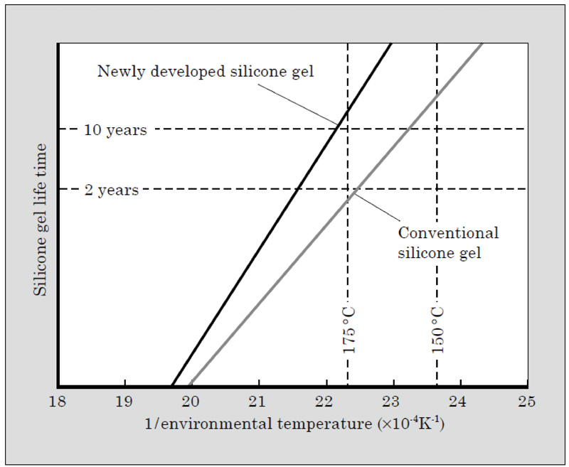
The relationship between temperature and silicone gel lifetime shown in Figure 6 clearly depicts the improvements in the 7th generation silicone gel. The conventional silicone gel could sustain a 10-year lifetime at 150ᵒC, however rapidly degraded to 2-year lifetime at 175ᵒC; the newly developed 7th generation silicone gel is able to sustain 10+year lifetime when operated at 175ᵒC.
Click image to enlarge
Figure 6: Relationship between silicone gel temperature and lifetime
The Fuji Electric 7th generation Dual XT 2:1 module is offered in standard configuration 225A, 300A, 450A, & 600A at 1200V & 1700V with Visol =2.5kV and 3.4kV respectively and resin-based case with a comparative tracking index range of 175≤CTI<250.
The Dual XT 2:1 premium configuration is available in 600A & 800A at 1200V and 600A at 1700V with Visol = 4KV and high comparative tracking CTI≥600 resin-based case material for demanding applications requiring high isolation and high tracking CTI, i.e. 1500V 3-Level NPC inverters. All 7th Dual XT IGBT modules are available with press-fit or solder pin connections.
Typical applications are in Renewable Energy: Wind Turbines and Solar Inverters; Industrial Drives for Factory Automation, HVAC, UPS, and etc.
We believe the 7th generation IGBT technology with reduced power dissipation made possible through the innovative technical enhancements of the semiconductor chip, improvements in current-carrying capability, and, improved thermal packaging design with the ability for sustained 175ᵒC Tvj(op) operation offers a powerful and compelling solution for power system designers seeking a high-efficiency and high-reliability solution for today’s demanding applications requirements.
In particular the 7th generation premium Dual XT 2:1 IGBT module provides a robust, highly efficient, and, high- reliability option to power today’s energy conversion systems.
References:
Kawabata, J. et al. 7th-Generation “X Series” IGBT Module. FUJI ELECTRIC REVIEW. 2015, vol.61, no.4, p.237-241.
Yoshida, K. et al. 7th-Generation “X Series” IGBT Module “Dual XT”. FUJI ELECTRIC REVIEW. 2016, vol.62, no.4, p.236-240.

