GaN Technology Breaks into Power Supply Designs
A look at the technological journey of the power supply and the rise of gallium nitride
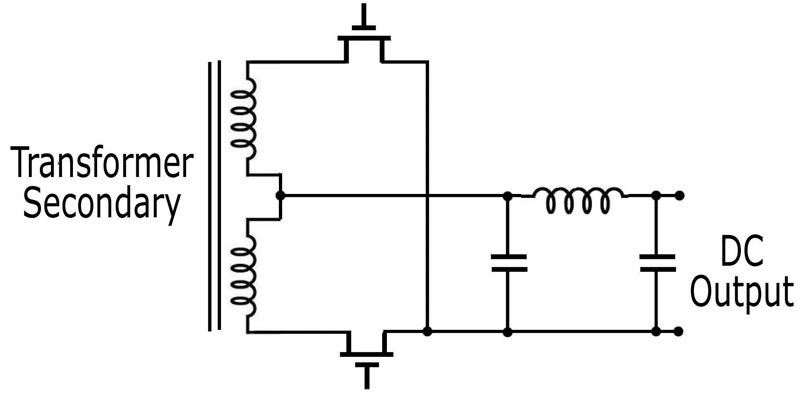
Figure 1: Synchronous rectification in a secondary circuit
The ideal AC-DC power supply will be compact, reliable and cool running. This has been the request from equipment designers in the industrial and medical industries since the dawn of the electronic age. With the advent of switch mode power supplies in the 1970s, the industry took a quantum leap towards this goal. Since then, there have been major design improvements as new technologies become available.
The size of the power supply depends mainly on how efficiently it operates - higher efficiency equates to less wasted heat, allowing the use of smaller heatsinks and filter components. A 75% efficient 1000W power supply, for example, will consume 1,333W to output 1000W, 333W of which will be losses. A 95% efficient product, on the other hand, will consume 1,053W with just 53W losses. If the power supply is too small, achieving the required amount of cooling becomes difficult. Internal temperatures may rise excessively, this makes the electrolytic capacitors dry out and semiconductor junction temperatures run too hot and, hence, shortens the service life.
The 1970s brought the introduction of switch mode power supplies into the mass production industrial market, replacing the bulky, narrow input range, heavy, inefficient linear supplies. Since then there has been a number of significant leaps in technology. High speed MOSFETs replaced the slower bi-polar power transistors, which increased the operating frequencies of power supplies from around 20 kHz to above 100 kHz. This reduced the size and losses of the power magnetics and filter components.
Electrolytic capacitor life went from 2,000 hours incrementally up to over 10,000 hours and surface mount technology and multiple layer printed circuit boards became affordable. New ferrite materials and core shapes for lower losses and higher frequency switching have also become available.
Synchronous rectification has now become common in the output rectification section of both AC-DC power supplies and DC-DC converters. In Figure 1, the low forward voltage drop Schottky diodes (which replaced silicon diodes) have been replaced by low resistance (RDSON) MOSFETs. Although the FETS require drive circuits, the improvement in efficiency and performance outweigh the additional complexity.
In the last decade, digital signal processors (DSPs) have now started to replace the traditional analogue control ICs. Digital control loops allow for better stability and gives the power supply designer more flexibility in developing new circuit designs. It also enables software modifications to, for example, allow start-up into large capacitive loads without changing component values and circuitry. Communication and programming functions have been added to some controllers to allow PMBus interfaces to be included in the power supply design.
Up until recently, power supply designers have been reliant on silicon-based power devices. While silicon Carbide (SiC) devices have replaced some silicon devices, another wide-bandgap (WBG) semiconductor, Gallium Nitride (GaN), is offering designers a new way of implementing even more efficient and lower cost circuits with 100V to 650V device ratings.
Transphorm Inc., a global semiconductor company and leader in GaN development, announced recently that it has now shipped more than 250,000 650V GaN HEMT (High Electron Mobility Transistor) devices and currently has a 15 million annual part capacity base. GaN’s success is driven by the opportunity to increase power supply efficiency and reduce size. Datacentres, military and equipment requiring fan-less operation, lower operating cost and smaller size have been early adopters of this technology. TDK-Lambda partnered with Transphorm Inc. during the development of its PFH500F series of 3rd generation 500W AC-DC conduction cooled power modules.
The design challenge was to reduce the size and increase the power conversion efficiency of the existing TDK-Lambda PFE series of AC-DC power modules. GaN HEMTs enabled TDK-Lambda to employ a bridgeless totem-pole power factor correction (PFC) topology, replacing the traditional full-bridge rectification topology. The PFC circuit converts the AC input into a regulated high voltage DC (typically 380 to 400Vdc). A DC-DC power converter then reduces the high voltage DC into a regulated low DC output voltage, with electrical isolation, typically between 5 and 48V.
Figure 2 shows a PFC circuit using diodes configured for full wave rectification. When the switching converter is powered, there are two diode drops in the rectifier part of the circuit and one diode drop in the boost stage, a total of three diode drops.
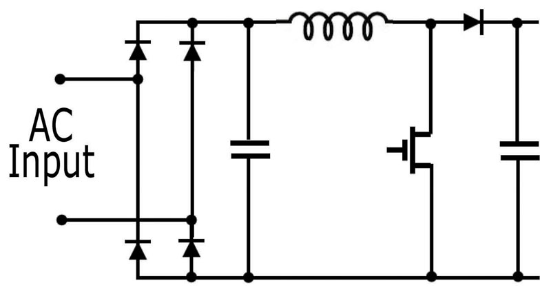
Click image to enlarge
Figure 2: PFC circuit using diode rectifiers
There is only 1 diode drop in the Totem-Pole PFC topology (fig 3). If the remaining line frequency diodes are replaced with Si FETs operating at AC line low frequency, then it will have no diode drop. Within the Totem Pole PFC topology, two of the slow diodes are replaced by GaN HEMT devices.
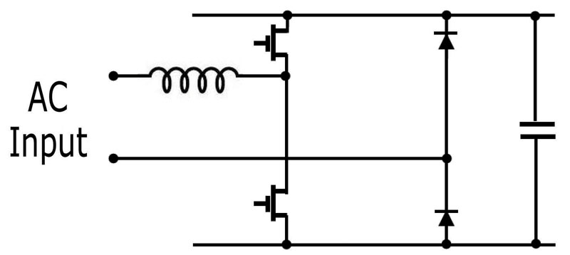
Click image to enlarge
Figure 3: Totem pole bridgeless PFC (two GaN HEMTs and two diodes)
Traditional silicon MOSFETs cannot be used in this manner because of their large reverse recovery charge and the high bus voltage. The DC bus voltage is always higher than the input AC line voltage at any given moment. Si FETs can only be considered for the Totem Pole PFC circuit operated in the discontinuous mode, which causes too much peak current in the switching devices, the boost inductor, and the input filtering components. EMI will be very difficult to manage.
When compared to the performance of the full featured PFE500F AC-DC power module, the gains are significant:

Furthermore, space savings allowed PMBus monitoring and programming (read/write) to be included.
When GaN technology first became available to the power supply industry, there was an awareness that there would be a requirement to proceed carefully with product development. Replacing a Silicon MOSFET with a GaN FET is not a simple task. Greater timing precision in the drive circuit is required and the switches are more sensitive to parasitic impedances from both inside the power supply and outside. Cost was also a concern, as the device’s usage has not been in the high volumes that are associated with Silicon MOSFETs.
Now that chip manufacturers are supplying easier to use gate drivers and controllers, power supply designers are gaining experience in using these GaN devices. Production volumes continue to increase and as more semiconductor manufacturers launch products, prices will no doubt drop. Increasing environmental concerns will mandate the need for higher efficiency products, which will lead to tighter government regulation. The age of GaN is happening.
TDK-Lambda