Gate Driver Choices for High Power Density Intermediate Bus Converters in AI Servers

Matching converter architecture, power-switch technology, and integration features to 48 V-class intermediate bus converters (IBC) requirements
Figure 1: Two-stage 48 V power architecture for an AI server, showing IBC and downstream point-of-load regulation
1. AI server power delivery raises the density challenge
AI accelerators concentrate more computing, and therefore more electrical power, within limited rack and board space. Supplying these loads is not simply a matter of increasing converter output. Every power‑delivery stage must balance conversion efficiency, power density, thermal performance, electromagnetic interference, and respond to rapidly changing demand.
Power enters servers through power supply units, while battery backup units may provide ride-through capability when required. From there, distributing power at a higher bus voltage limits current and associated conduction losses. The voltage is then stepped down close to processors, where space and cooling capacity are constrained.
This architecture places greater demands on intermediate conversion. Its topology, power switches, gate drivers, magnetics, capacitors, control, and layout must work together as a system. Gate‑ selection is therefore critical for an efficient and compact converter.
2. The role of the intermediate bus converter (IBC)
In a typical AI server power architecture, the IBC bridges the gap between the higher-voltage distribution bus and the low-voltage rails required by processors and other board-level loads. For a 48 V-class distribution system, the IBC steps the bus voltage down to a level that downstream point-of-load regulators can convert with precise regulation and fast transient response. This division of work optimizes each conversion stage for a specific function.
An IBC provides regulated conversion or operates as a fixed-ratio DC transformer using buck-derived, multilevel, and switched-capacitor topologies depending on the required conversion ratio, load range, control method, available board area, and balancing switching and conduction losses.
The IBC must also operate within the thermal and spatial constraints close to high-power computing devices. Increasing switching frequency reduces passive-component size, but raises switching, gate-drive, magnetic, and layout-related losses. Higher power density requires coordinated selection of topologies, power switches, gate drivers, passive components, control strategy, and PCB layout rather than optimization of components in isolation.
3. Why the gate driver matters
The gate driver connects controller signals to power switches, but its role extends beyond translating voltage levels. It must charge and discharge switch gates with controlled timing and sufficient current while coordinating between switching channels. These requirements become more demanding in IBCs using multiple switching nodes, floating voltage domains, or closely timed transitions.
The converter architecture establishes the required channel arrangement. A conventional half-bridge may use high-side and low-side outputs, while multilevel and switched-capacitor topologies require independently controlled floating channels. Trying to match propagation and channel-to-channel delays impacts transition timing. Source and sink capability influence how quickly a switch turns on and off, while dead-time control coordinates complementary devices.
Other functions can be equally important. Adjustable drive strength supports controlled startup behavior. Integrated current sensing reduces separate signal-conditioning circuitry when its sensing matches the control architecture. Supply-voltage range, undervoltage lockout, input logic, negative-voltage tolerance, and package dimensions also matter.
Technology also matters. Silicon MOSFETs and enhancement-mode GaN transistors have distinct gate‑voltage, switching, thermal, and layout characteristics. Designers should evaluate driver-switch combinations against topologies, operating conditions, switching-frequency targets, thermal constraints, control strategies, and system priorities.
4. Dual-floating control with 2EDL6014AC-G2D
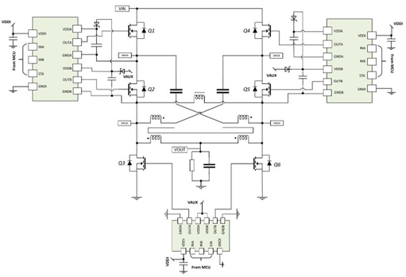
Multilevel and switched-capacitor converters can have switches at different voltage potentials, creating drive requirements that are not always served efficiently by conventional high-side and low-side drivers. EiceDRIVER™ 2EDL6014AC-G2D addresses this with two independently controlled, junction-isolated floating output channels that drive dual-high-side, dual-low-side, or half-bridges, helping implement several IBC topologies with one architecture.
Each channel provides up to 4 A source and 6 A sink current. A typical propagation delay of 20 ns and typical channel-to-channel delay matching of 1 ns support closely coordinated switching. The 4 V to 16 V gate-supply range accommodates different low-voltage MOSFET drive requirements, while the 2.2 mm × 2.2 mm package supports compact placement near switches. The driver offers optimized thermal performance because the package has an exposed thermal pad resulting in low thermal resistance (Rth‑jc(bottom)) of 4.1 K/W.
Startups are challenging in switched-capacitor and multilevel converters because uncontrolled capacitor‑charging current imposes substantial stress on the power stage. Source-current adjustability allows OUTA peak source current to reduce from 4 A to 500 mA. This slows switch transition during startup while retaining higher drive-current settings for normal operation.
The EVAL_HB_2EDL6014AC evaluation board uses OptiMOS™ 80 V MOSFETs in a hard-switching half‑bridge supporting both common-ground and voltage-level-shifted operation, allowing examination of driver and power-switch waveforms under different supply voltages from 36 V to 60 V for a 15 A load at 200 kHz switching.
Click image to enlarge
Figure 2: 2EDL6014AC-G2D dual-floating-channel application arrangement
5. Configurable Si and GaN driving with 2EDL90xG3
IBC development requires evaluating silicon MOSFETs and GaN transistors against the same PCB. The EiceDRIVER™ 2EDL90xG3 family supports this through two variants in a common 3 mm × 3 mm package. 2EDL900G3 provides 4 A source and 6 A sink for silicon MOSFETs, while 2EDL901G3 provides 1.6 A source and 6 A sink with a 5 V gate clamp for GaN transistors.
The family supports several control arrangements: tri-state single-PWM operation, independent high-side and low-side inputs, inverted inputs, or operating modes intended for hybrid switched-capacitor converters. Configurable dead-time or turn-on delay from 6 ns to 100 ns allows coordinating switching transitions with selected topologies and power devices. The two floating output channels support half-bridge, multilevel, hybrid switched-capacitor, and other switched-capacitor implementations.
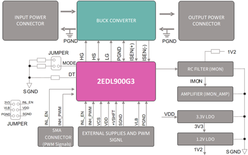
An integrated current-sense amplifier supports inductor DCR current sensing or shunt resistor based current sensing that can be used for converter control loops, monitoring, or protection without a separate current-sense amplifier. Designers should account for signal bandwidth, thermal variation, accuracy requirements, and PCB implementation when defining the measurement path.
The EVAL_HB_2EDL900G3_Si evaluation board demonstrates the silicon-driver variant with OptiMOS™ 80 V MOSFETs for tri-state single-PWM and independent high-side/low-side input modes, to observe integrated current-monitoring signals, and board configurations for common-ground or voltage-level-shifted operation. Evaluations include gate-switching and current-monitoring waveforms at input voltages from 36 V to 60 V and a load current of 15 A.
Click image to enlarge
Figure 3: 2EDL900G3 evaluation platform block diagram
6. Compact half-bridge driving with 2EDL501xAA-U2D
For IBC implementations based on conventional half-bridges, the EiceDRIVER™ 2EDL501xAA-U2D family provides compact driver architectures for GaN transistors and logic-level silicon MOSFETs. The family comprises three variants:
- 2EDL5011AA-U2D with 1.5 A source and sink
- 2EDL5012AA-U2D with 1.5 A source and 4 A sink
- 2EDL5014AA-U2D with 4 A source and sink
This range allows matching drive strength to selected power switches and switching-transition targets.
An integrated bootstrap switch supplies the floating high-side channel. Active control prevents the bootstrap capacitor from overcharging during dead-time, particularly relevant when driving GaN transistors with restricted gate-voltage ranges. Split outputs provide separate paths for adjusting turn-on and turn-off drive strengths, while active Miller clamps on both channels help prevent induced turn-on during switching transitions.
The devices operate from a 4.5 V to 5.5 V supply and are offered in a 2 mm × 2 mm TSNP-12 package, making the family a focused option for compact half-bridge power stages requiring independently tunable switching without additional configurations or integrated current sensing.
7. Selecting the driver around the converter
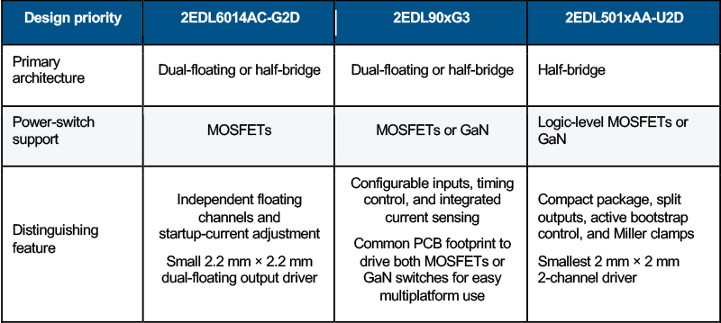
Gate driver selection starts with the converter’s channel architecture. Multilevel and switched-capacitor topologies benefit from independently controlled floating outputs such as those provided by 2EDL6014AC-G2D. Designs requiring configurable inputs, integrated current sensing, and a platform path for either silicon or GaN can use the capabilities of the 2EDL90xG3 family. Conventional half-bridges requiring compact placement and independently adjustable turn-on and turn-off paths can be addressed with the 2EDL501xAA-U2D family.
The next step is to match the driver’s supply range, output current, timing, control modes, and protection‑related functions to the selected power switches. MOSFETs and medium-voltage GaN transistors provide useful characteristics for IBC power stages. Their system value emerges through coordinated selection of switching frequency, thermal design, magnetics, control, layout, and gate drives.
Evaluation platforms for 2EDL6014AC-G2D and 2EDL900G3 provide a practical starting point for examining switching waveforms, supply-reference configurations, control modes, and current-monitoring behavior. Designers can then validate the selected driver-and-switch combination under the electrical, thermal, and transient conditions of the target converter.
Click image to enlarge
Table 1: gate driver selection guide