The 800 V GaN Transition and the Protection Ecosystem

How high-bandwidth current sensing and fast gate driving enable reliable sub-500 ns protection in EV power conversion
Figure 1: Simplified comparison of a traditional two-level SiC power stage and a three-level multi-level GaN topology
The shift to 800 V electric vehicle (EV) power architectures is about more than just voltage rating. Moving to multi-level gallium nitride (GaN) topologies can improve system cost, thermal performance and power density compared with traditional high-voltage silicon carbide (SiC) approaches. By dividing voltage stress across lower-voltage devices, a GaN-based approach can reduce switching losses, shrink the size of passive components and support more compact power conversion in on-board chargers (OBCs) and DC-DC converters.
However, realizing these advantages requires a protection chain that is fast enough. In high-speed GaN power systems, current sensing and gate driving are no longer simply supporting functions but core enablers of reliable operation.
The Evolution of 800 V Architectures
The shift from 400 V to 800 V EV platforms is driven by the need for faster charging, higher efficiency and improved power density. Raising the voltage reduces current for a given power level, helping to cut conduction losses and reduce cable size. For high-performance EVs, 800 V architectures are therefore becoming an important route to faster charging and more efficient energy management.
The first phase of this transition has largely been enabled by SiC MOSFETs, which are well suited to high-voltage power conversion and have helped make 800 V systems practical. However, conventional two-level 800 V SiC designs can carry cost, thermal and packaging penalties. High-voltage SiC devices remain relatively costly, and dense charger designs still need careful management of heat, EMI and passive component size.
Multi-level GaN architectures offer an alternative:instead of relying on a single high-voltage device to block the full DC-link voltage, multi-level topologies distribute voltage stress across multiple lower-voltage switches. This allows designers to use lower-voltage GaN FETs, such as 400 V or 650 V devices, in 800 V OBC and DC-DC converter designs. The result is an architectural change that can improve efficiency and bill of materials (BoM) cost, while also introducing new requirements for thermal design, control strategy and protection timing.
Efficiency and BoM Benefit
GaN’s attraction lies in its ability to switch rapidly with low switching power losses. Higher switching frequency allows designers to reduce the size of magnetics and capacitors, as less energy is needed to be stored in each switching cycle. This is especially valuable in Evs, where power density directly affects package size, weight and system integration.
Multi-level topologies strengthen this benefit by addressing the voltage-rating problem. The design can use lower-voltage GaN devices by sharing the 800 V bus across several switching nodes, instead of relying solely on 1200 V-class SiC components. In the right architecture, this can improve the total cost/performance balance of the power stage.
Faster switching can reduce losses and ease thermal design. More compact conversion stages enable lighter mechanical assemblies and more integrated charger layouts. Together, these factors help address the cost and weight penalties associated with some high-voltage SiC implementations.
However, these gains are not automatic – multi-level GaN increases the number of switching nodes and places greater demands on current sensing, isolation and gate-drive precision. The faster and denser the design becomes, the less tolerance it has for slow protection or imprecise measurement.
It is also worth noting that the long-term robustness of GaN in automotive is still a developing story – and GaN is still evolving, particularly compared to the more established SiC ecosystem.
The Critical Failure Narrative
Moving from SiC to GaN also changes the fault profile of the power stage. SiC devices are not immune to overcurrent or short-circuit events, but many SiC-based designs can tolerate faults over microsecond-scale windows, depending on device type, operating conditions and protection strategy. That gives the system a short but usable interval to detect the event and shut down safely.
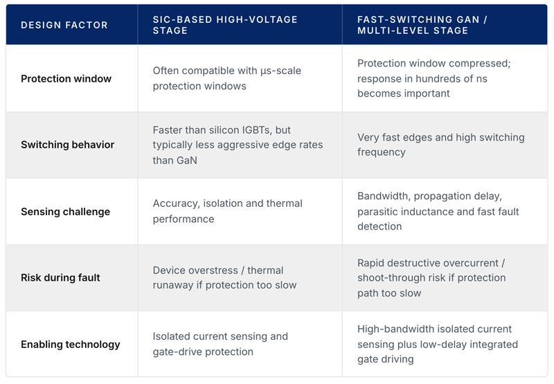
GaN reduces that margin, and the same characteristics that make GaN attractive — small die size, fast edges and very high switching speed — also compress the available protection window (see Table 1). In a compact, high-density GaN power stage, a shoot-through event, short circuit or abnormal current spike can become destructive extremely quickly.
Current sensing can no longer be treated as a relatively slow monitoring function. In high-frequency wide bandgap (WBG) systems, it becomes part of the real-time protection and control loop. If sensing, isolation or gate-drive response is too slow, the theoretical advantages of GaN are compromised.
Designers may then be forced to add margin elsewhere: larger devices, heavier filtering, slower switching edges, more conservative derating or additional thermal capacity. That undermines the very reasons for adopting multi-level GaN. The real challenge is therefore not only to select the right power switch, but to build a protection ecosystem fast enough to make the architecture viable.
Click image to enlarge
Table 1: Comparison of protection considerations in SiC and fast-switching multi-level GaN power stages
Why Sub-500 ns Protection Matters
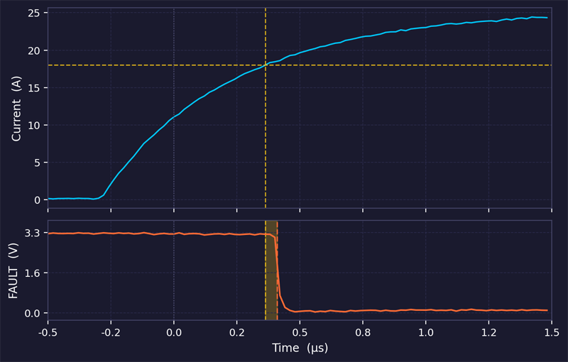
For fast-switching GaN power stages in 800 V OBC and DC-DC converter applications, protection timing becomes a defining design parameter. In many such power stages, designers target a total overcurrent response below 500 ns from detection to action. This is not only a sensor specification, it is a system-level timing budget covering sensing bandwidth, signal integrity, propagation delay, decision logic and gate-driver turn-off behaviour.
Current measurement is the first link in that chain. Traditional shunt-based sensing remains widely used and offers high accuracy, but becomes harder to implement cleanly at high current, high voltage and high switching frequency. The shunt introduces power loss, while the surrounding layout adds parasitic inductance. Isolation, filtering and signal conditioning can also add delay or limit usable bandwidth. At GaN edge rates, these effects become significant.
Integrated magnetic sensing provides another route. Hall-effect and tunnel magnetoresistive (TMR) current sensors deliver isolated current measurement without inserting a lossy shunt into the main current path. By reducing insertion loss and avoiding some of the parasitic and thermal compromises of high-current shunts, they can support faster and cleaner fault detection in WBG systems.
This is where Allegro’s Hall-effect and TMR current sensors become important, by providing isolated, high-bandwidth current measurement for power-conversion systems where protection timing and control accuracy are increasingly critical. TMR technology, in particular, offers high sensitivity, low noise and very fast response. In a GaN-based power stage, that allows current sensing to move from supervisory monitoring into the core protection and control architecture.
The gate driver is the second part of the chain: in a multi-level topology, the driver must manage multiple switching nodes, maintain isolation, minimize propagation delay and support precise timing control. Integrated isolated gate drivers help by combining the gate-drive function with isolated bias supply capability, reducing reliance on external isolated supplies, bootstrap circuitry and associated passives. This simplifies layout, reduces component count and lowers common-mode capacitance — all important in high-speed WBG systems.
Together, fast isolated current sensing and integrated isolated gate driving create the practical protection path required by multi-level GaN. The sensor detects the fault quickly and accurately, while the gate driver executes the shutdown with predictable timing. By combining high bandwidth, low propagation delay and isolation, the sensing path reduces protection latency and improves timing predictability from detection to shutdown. Without both elements, a sub-500 ns protection target becomes much harder to achieve.
Click image to enlarge
Figure 2: Fault response timeline – detection to shutdown (<500 ns)
System-Level Impact: Optimizing Design
As well as preventing device failure, fast protection influences how the rest of the system can be designed, enabling smaller, lower-cost power converters.
When designers do not trust the protection chain, they compensate with margin. They overspecify switches, increase thermal capacity, add filtering, slow switching transitions or derate the operating envelope. In safety-critical automotive systems, these choices are understandable, but they add cost, size, weight and complexity.
A faster sensing and gate-driver ecosystem allows those margins to be reassessed. If an overcurrent event can be detected and acted on within a tightly controlled timing window, the power stage need not be designed around the assumption of prolonged fault exposure. In turn, this enables a design to support more optimized device selection, tighter thermal design, smaller passive components and more compact layouts.
There are also control benefits, because high-bandwidth current feedback enables tighter control loops, faster transient response and improved optimization of switching behavior. In multi-level GaN designs, where several nodes must be coordinated precisely, measurement fidelity becomes central to stable operation.
For automotive OBCs and DC-DC converters, this is increasingly linked to functional safety and diagnostic coverage. As power density rises, integrated sensing and gate driving will be judged less as optional performance enhancements and more as infrastructure that enables robust, manufacturable designs.
Conclusion and Future Outlook
In the next phase of EV charging design, SiC will remain important in high-voltage power conversion, but multi-level GaN offers a compelling route for selected 800 V OBCs and DC-DC converters where higher density, lower system cost and improved thermal performance are priorities.
The challenge is that GaN compresses the protection window. Faster switching, smaller devices, and more complex switching nodes mean that sensing and gate driving must evolve at the same pace as the semiconductors themselves.
High-bandwidth isolated current sensors and integrated isolated gate drivers are becoming essential parts of the 800 V GaN ecosystem. By enabling fast detection, clean isolation, simplified gate-drive design and predictable shutdown, they are important enabling technologies for multi-level designs – and fast sensing and protection technologies will be essential complementary enablers for broader deployment of multi-level architectures.
As EV platforms move toward higher charging power, greater integration and tighter cost targets, the winning designs will combine fast switches with equally fast, reliable and integrated protection paths.