High-speed photocouplers have integrated IGBT protection function
High-speed photocouplers have integrated IGBT protection function
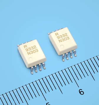
Targeting applications such as industrial machinery and solar power systems, the PS9332L and PS9332L2 photocouplers from Renesas Electronics have an integrated insulated-gate bipolar transistor (IGBT) protection function. The devices also feature an integrated active Miller clamp circuit to prevent IGBT malfunction, high-speed switching (20 percent faster than conventional products) among IGBT drive photocouplers with integrated IGBT protection function, compact 8-pin SDIP (shrink dual inline package), and guaranteed high-temperature operation. The photocouplers can be used for gate drive of IGBT devices used in inverter circuits for motor control, etc. The PS9332L and PS9332L2 are IGBT drive photocouplers consisting of a gallium-aluminum-arsenide (GaAlAs) LED as the light emitting diode, photo detector IC, and an IGBT protection circuit. They are designed to drive the gate of an IGBT device while at the same time providing an integrated protection function (active Miller clamp) to prevent destruction due to malfunction of the IGBT. In a conventional system this protection function must be implemented by means of external components, resulting in a more complex system design and making miniaturization difficult. The PS9332L and PS9332L2 solve this problem. Key Features: 1) On-chip active Miller clamp circuit to prevent IGBT malfunction When the IGBT connected to the photocoupler turns off, current flow (Miller current) between the collector and gate can cause a gate voltage, resulting in malfunction. The integrated active Miller clamp circuit shortens the gate charge to ground, suppressing any rise in the gate voltage and preventing malfunction. Integrating the protection circuit into the photocoupler simplifies system design and enables the system to be more compact overall. 2) High-speed switching (20 percent faster than conventional Renesas products) The photo detector IC uses Renesas' exclusive BiCMOS process, resulting in low parasitic capacitance [Note 3], shorter delay time (tPHL, tPLH ? 200 ns, 20 percent less than comparable earlier products), and low current consumption by the circuit (Icc ? 2.5 mA). This makes it possible to build inverter control circuits that are more precise and have lower power consumption. In addition, the circuit's low current consumption enables a more compact power supply for the system driving the IGBTs. 3) Compact 8-pin SDIP package Although it now includes an integrated active Miller clamp function, the size of the photo detector chip is equivalent to that of comparable earlier products, allowing a compact 8-pin SDIP package. This provides a 40 percent reduction in mounting area compared with an 8-pin DIP, allowing customers to build more compact systems. The package is available with two lead frame options. The PS9332L offers 7 mm outer creepage, whereas the PS9332L2 offers 8 mm. 4) Guaranteed high-temperature operation The materials have been improved to allow operation at high temperatures, for a maximum operating ambient temperature of 125 degrees C. This simplifies the thermal design of systems in hot environments. The PS9332L and PS9332L2 can simplify development of and allow greater compactness in inverter products, the market for which is expected to grow moving forward. While expanding sales promotion aggressively, Renesas will continue to develop new products with support for the high-temperature, high-speed, and high-output requirements of customers. Using the new products in combination with Renesas' IGBT can reduce dead time in switching by about 10 percent (compared with conventional products) and improve power efficiency. Also, Renesas expands support of customers' product development with reference boards for devices such as power conditioners and inverters as kit solution with MCUs. Renesas Electronics Europe