How SiC and GaN Enable Higher Power Conversion Efficiency
SiC and GaN technologies have characteristics that must be considered to extract maximum benefit, but fewer losses knock-on to other valuable benefits
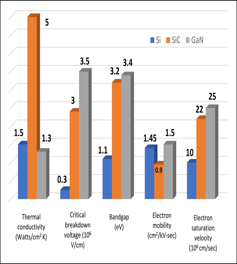
Figure 1: Main differences between Si, SiC and GaN materials
Energy usage and its conversion from source to final application has been a subject of development ever since horsepower meant exactly that, and the design of a plough was critical to how many days it would take to prepare a field for planting. Today we think more about electrical energy and power conversion from a generator output to an end-voltage for a host of applications, be it 0.6VDC for a processor, 24VDC to 500VAC for an industrial motor drive or 400VDC to charge an EV battery. The conversion process invariably uses power semiconductor switches and silicon-based types have been dominant for decades in the form of Si-MOSFETs and IGBTs. Losses in these switches are a major contribution to system inefficiency, and, today, reducing power wastage has become a focus to minimise operating costs and the burden on the environment.
In recent years, alternative materials to silicon have become viable, in the form of Silicon Carbide (SiC), and Gallium Nitride (GaN), which have characteristics that enable step improvements in efficiency of power conversion. These wide band-gap (WBG) devices are not a simple substitution for Si though and application circuits must be designed to match, especially if the full performance benefits are to be extracted. Figure 1 shows the main differences between the materials.
Si, SiC and GaN –conduction losses
Si-IGBTs, have a minimum on-state collector-emitter saturation voltage which, with collector current, sets conduction losses. Si-MOSFETS have an on-state resistance so power dissipated is I.R(ON)2 which can be prohibitive at high current levels. At low voltage and low to medium power, however, Si-MOSFETs with low R(ON) can have lower conduction losses than IGBTs. SiC and GaN devices have a much higher critical breakdown voltage than Si, allowing a thinner drift layer and high doping concentration. This leads directly to lower on-resistance for a given die area and voltage rating, with consequent lower loss. Additionally, SiC has a thermal conductivity more than three times better than Si, so smaller die can be used for the same temperature rise. Both SiC and GaN anyway have much higher maximum operating temperatures than silicon, limiting stress.
Si, SiC and GaN –switching losses
High converter switching frequency is desirable, as associated components can be smaller, particularly magnetics, yielding savings in size, weight and cost. However, switching losses in all devices scale directly with frequency. IGBTs are rarely operated above 20kHz due to power lost due to ‘tail current’, necessary snubbers and charge and discharge of high device capacitances. Si-MOSFETs can switch at hundreds of kHz but energy lost, EOSS, in circulating current to the output capacitance becomes a limiting factor as frequency rises. SiC and GaN, however, have much higher electron saturation velocity and much lower capacitances, so can switch at high speed with low loss.
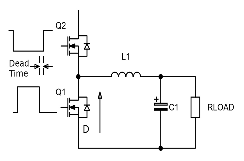
Also important are the characteristics of the devices in the ‘third quadrant’- when the conducting channel is reverse biased, as occurs in ‘hard switching’applications and when ‘commutation’happens in inverters (Figure 2). IGBTs do not conduct in reverse so an anti-parallel diode is required, which must be a fast recovery type with a low voltage drop. Si- and SiC-MOSFETS have inherent fast body diodes but can conduct through their channels in reverse with low loss and no reverse recovery effect when switched ON via their gates. Any ‘dead time’however when the channel is reverse biased but not set ON via the gate causes the body diode to conduct, with significant power lost because of its relatively high forward voltage drop. GaN switches are configured as HEMTs, High Electron Mobility Transistors, and have no body diode. Like MOSFETs, their channels can conduct in reverse but there is also a body diode effect through the channel during any dead time, with a voltage drop approximately equal to the gate threshold voltage, around 2V. This again can cause dissipation unless the channel is actively turned ON.
Click image to enlarge
Figure 2: A hard switched synchronous buck converter forces body diode D to conduct during ‘dead’ times
Practical implementation of SiC and GaN devices
Operating maximum voltages are a main consideration for the different switch technologies; the maximum for high power Si-MOSFETs is around 950V, for GaN HEMTs it is 600V and SiC MOSFETs around 1700V. IGBTs are still dominant at very high voltages although MOSFETs can be ‘stacked’in some topologies to reduce voltage stress. When over-voltage does occur, IGBTs and MOSFETS have a protective avalanche mode with different device-dependent energy ratings. GaN HEMTs do not have an avalanche mode and therefore physically break down catastrophically under voltage over-stress. GaN device manufacturers therefore make sure that there is a large margin between datasheet rated and absolute maximum voltages.
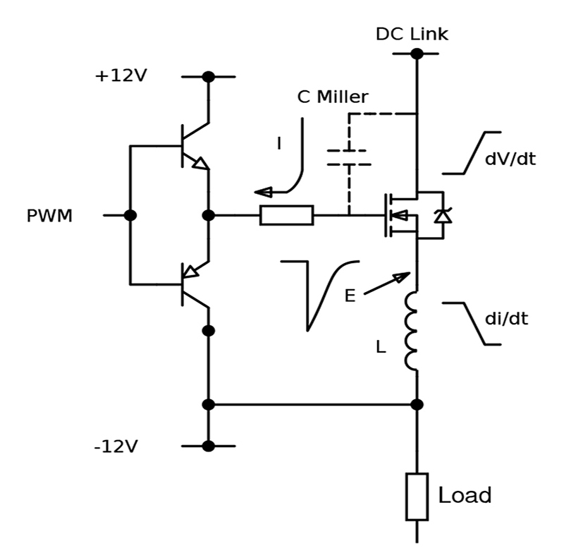
Optimum gate drive arrangements are quite different between device technologies. Si-IGBTs have insulated gates but high total gate charge requiring significant drive power, scaling directly with gate voltage swing and frequency, so that the largest devices need several watts at realistic switching frequencies. Si-MOSFETs have much lower gate charge and lower drive power requirements and, like IGBTs, have a gate threshold voltage of around 10V for full enhancement. Absolute maximum gate voltage is typically +/-25V. The gate is often driven to a negative voltage, up to around -12V, to switch the device OFF. This is to counter the effects of ‘Miller’capacitance and any common inductance in the source/emitter connection, both of which tend to produce transients which oppose the OFF-state gate drive (Figure 3).
Click image to enlarge
Figure 3: Negative gate drive counters effect of Miller capacitance and source inductance transients
SiC and GaN, particularly, have extremely low total gate charge and insignificant drive power requirements. SiC gates must be driven to nearly 20V however for full enhancement, close to the typical absolute maximum of +25V. Protection clamp diodes are therefore often introduced to avoid voltage stress. GaN HEMTs are actually current driven with a voltage of around 3V producing the few mA required to turn the device fully ON. The voltage varies strongly with temperature and drain current so is not normally specified as a threshold VTH. A maximum gate current is therefore specified, measured in tens of mA, although amps of pulsed current are allowed dependent on pulse width and repetition rate. Both SiC and GaN can also suffer from ‘phantom’turn on due to the inherent extremely high di/dt and dV/dt levels seen, so a few volts of negative gate drive are often proposed for the OFF-state. GaN devices are particularly at risk with their low effective threshold voltage and fastest dV/dt. Device manufacturers however commonly provide SiC and GaN parts with ‘Kelvin’connections to the source so that the gate drive loop can be effectively separated from the main current path, reducing or eliminating the problem. Driving GaN HEMT gates negative can be problematic as the voltage directly adds to the body diode effect drop, if the channel conducts in reverse during ‘dead’times, increasing dissipation.
Gate drives for SiC and GaN devices will typically include extra series resistance to deliberately slow switching edge rates as a compromise between EMI and efficiency. Circuits with separate resistance for ON- and OFF-drives are common using steering diodes.
Applications for SiC and GaN
SiC is now common in power applications with 650V to 1700V ratings matching common single- and three-phase industrial and inverter levels. The devices are proven to be rugged and state-of-the-art driver devices and techniques are making them even more widely applicable. SiC devices can be retro-fitted to some existing applications using Si-MOSFETs or even IGBTs with some modifications to drive techniques and snubbing, but ground-up designs taking advantage of higher switching frequencies using appropriate layout techniques can give more benefit with smaller associated magnetic components.
GaN devices are finding increasing use in power supplies where the GaN devices offer the best efficiency performance in lower voltage applications such as solar inverters, telecomms DC-DC converters, class D audio amplifiers and in single phase AC power supplies. Concerns about sensitivity to drive levels are addressed by ‘cascode’configurations with gate characteristics that are equivalent to Si MOSFETs. After initial reservations about proven device reliability, the technology is now mature and failure mechanisms understood, so the parts can be designed-in with confidence, taking account of absolute maximum ratings. Rated voltages for GaN are set to increase anyway in the future, so they will increasingly compete with SiC- and Si-MOSFETs at around 900-1000V, which is a major application area for industrial DC levels and higher battery voltages in electric vehicles.
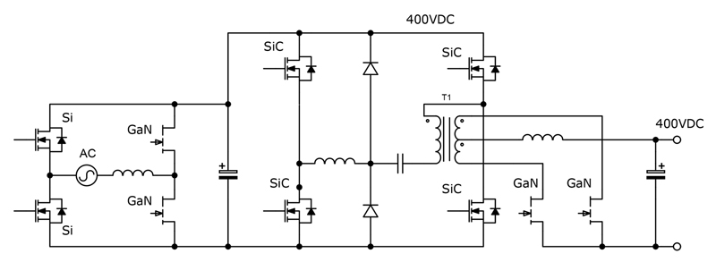
SiC and GaN can be used to advantage in all stages of a typical power converter from totem pole rectifier PFC stage through main inverter to synchronous output rectifiers (Figure 4).
Click image to enlarge
Figure 4: SiC and GaN can be used throughout a typical power converter


