How to Cancel Ambient Light for LIDAR Receivers
One of the more difficult challenges of time of flight (ToF) LIDAR is the high sensitivity required for the receive signal chain
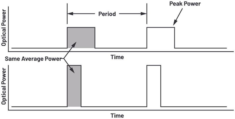
Figure 1: Example of different laser outputs
LIDAR works by using a laser to send out a narrow pulse of light, which hits a target, and the light reflects back. A detector measures the time the reflection takes to return. By knowing the speed of light and round trip time of the laser pulse, the distance can be calculated. Generally, the higher the amplitude of the pulsed laser, the larger the return signal. For long-range LIDAR, eye safety from the power of the laser limits the range. The area under the curve dictates the energy of the pulse, as shown in Figure 1. By going to higher peak power, the width of this pulse must be reduced to keep the area under the curve. In current LIDAR systems, the pulse widths are on the order of 5ns and are getting shorter. Another aspect to consider for LIDAR is scattering. Typically, an avalanche photodiode (APD) detector provides optical gain to combat the inverse square law problem. APDs are beneficial for the signal chain, since the transimpedance amplifier (TIA) is the limiting factor for noise in the signal chain. Gain applied in the detector reduces the system’s input referred noise. Too much gain in the APD will produce worse noise performance as it reaches breakdown.
LIDAR challenges
The receive signal chain needs to have high enough bandwidth to detect the edges of ~5 ns widelaser pulses, and the capacitance of the detector needs to be small to not limit the TIA bandwidth. The smaller capacitance also helps the shot noise of the APD since they are proportional to one another. Sensitivity, bandwidth, and power must be balanced. Another challenge of having higher gains in the receive signal chain is the large dynamic range that it brings. Modern APDs are reverse biased close to 300 volts to achieve these larger gains. The problem becomes apparent when a highly reflective object is very close to the detector. This large signal compounded with the relatively large gain of the APD can cause hundreds of mA to flow through the TIA. Most communications TIAs are not designed to survive this, let alone recover within a reasonable time for the next pulse. Fortunately, LIDAR-specific TIAs have built-in clamps to shunt the current and recover under 100ns. Power is addressed by duty cycling and shutting down unused channels. The last big problem is the DC photo currents from the ambient light, and solving this is not trivial.
AC-coupled vs. DC-coupled input
At first glance, a simple solution would be to AC couple the inputs to the TIA to block the DC current. Unfortunately, there are many pitfalls with this approach. The saturation recovery time will be compromised, blinding the system. In the event of a large pulse from a close object, the AC capacitor will be charged. The TIA can only inject a small amount of current into the AC cap because the feedback resistors limit the current. Depending on the value of the capacitor, the RC time constant is very large and can take hundreds of µs to recover. This is unacceptable, since typically 2 µs of time is allocated for 100 m detections, and the signal from farther objects is missed. Another pitfall of AC coupling the TIA is the repetition rate of your laser source. When the incoming pulses are AC coupled, they will be averaged on the AC cap. The detector’s signal is unipolar and will slowly charge the AC capacitor. There will be a DC offset produced on this capacitor. This systematically reduces the linear range of the TIA, and the DC offset will change based on repetition rate and amplitude of return signal. Fortunately, a DC-coupled input avoids all these nuances and secondary effects, but adds complexity. An effective method for canceling this current is by incorporating a closed-loop circuit to inject opposite current into the input of the TIA.
DC cancel circuit
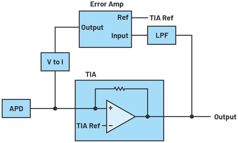
Figure 2 shows a block diagram of how to implement an analog closed loop tocancel DC input currents. The error amp looks at the output ofthe TIA and injects an opposite current into the TIA’s input. It compares and serves the output to match the TIA’s reference. It is best to use the TIA’s reference to derive the error amp’s reference to match the output’s reference, and to ensure the PSRR is conserved for the TIA. To save on powerand cost, a lower bandwidth amplifier should be used for the error amplifier’s circuit. Alow-pass filter is recommended for the error amplifier’s input since fast pulses can couple back to the input.
Click image to enlarge
Figure 2: DC cancel block diagram
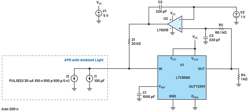
Figure 3 shows the DC cancel circuit for the LTC6560. Nominally the output of the LTC6560 sits about 1VDC when there is no input current into the TIA. Therefore, a resistor divider is needed from the reference to match this voltage, dividing down the reference nominal 1.5V to match the output 1V. R1 and C1 create a low pass of about 10.6 kHz to help minimize the amount of noise injected into the LTC6560 from the error amplifier. This low pass will be the dominant pole for this loop and can be adjusted for different bandwidth requirements. A simple integrating error amplifier circuit is used to servo the output of the LTC6560 to 1 V; 1 V is the nominal output voltage when there is no current on the LTC6560. R2, a 20 kΩ resistor, converts the LT6015’s output to a current. The value of this resistor and the maximum swing of the op amp will set the max current based on the LT6015 output swing. Since the LT6015 is not a rail-to-rail op amp, the max DC current cancel is limited to the difference between the max swing of the LT6015 and the input self-bias voltage of the LTC6560, which is nominally 1.5 V. This works out to be about 3V and will give a maximum DC cancel current of 150 µA.

Click image to enlarge
Figure 3: DC cancel circuit for the LTC6560
Figure 4 and 5 show an LTspice simulation of the LTC6560 DC cancel circuit. V2 is used in the simulation to set the reference of the integrating error amp. This helps the circuit simulate and establish a deterministic starting voltage.
Click image to enlarge
Figure 4: LTspice simulation schematic

Click image to enlarge
Figure 5: Input and output waveform of the DC cancel simulation
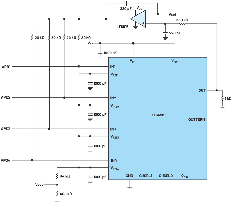
This DC cancel circuit can also be used with the LTC6561. Three LT6015s can be saved by using four output resistors to inject the current into each channel, shown in Figure 6. A path is created that cancouple the channels. However, 40 kΩ of resistance has a minimal impact onchannel-to-channel isolation. Lastly, the channels should be very similar in DCinput currents since the error amp cannot change drastically between channels.
Click image to enlarge
Figure 6: DC cancel circuit for the LTC6561
Results
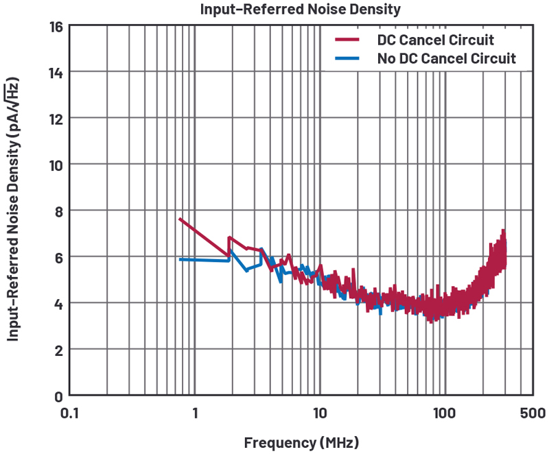
A proof of concept board was made to verify performance. The DC cancel circuitis dominated by the parasitic elements of the board routing and components. The circuit increases the integrated noise from 64 nA rms for the non-DC cancel circuit to 66nA rms for the DC cancel circuit integrated from 100 kHz to 200 MHz. Figure 7 shows the measured input referred noise densities with and without the DC cancel circuit. The APDs were removed from this circuit to find the noise floor without the capacitive loading to the TIA. This produced an integrated noise of 59 nA rms for the non-DC cancel circuit and 60 nA rms for the DC cancel circuit. The circuit is intended to be used with a detector and should include the capacitance into the performance of the circuit.
Click image to enlarge
Figure 7: The measured input referred noise densities with and without the DC cancel circuit