Figure 1: Simple schematic of the isolated gate driver ADuM4135
In power electronics, as found, for example, in drive technology, IGBTs are frequently used for high voltage and high current switching. These power transistors are voltage controlled and produce their main losses during switching. To minimize the switching losses, it is desirable to have short switching times. However, fast switching simultaneously conceals the danger of high voltage transients, which could possibly affect or even damage the processor logic. Hence, gate drivers that supply the IGBTs with the appropriate gate signals perform the function of providing short-circuit protection and influence the switching speed. However,in the selection of the gate driver, certain characteristics are critical.
Current-Driving Capability
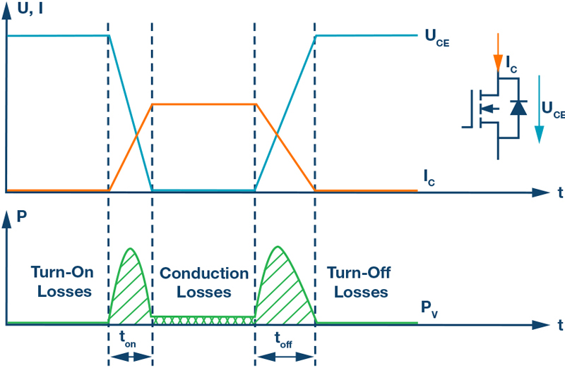
During switching, the transistor is briefly in a state in which both a high voltage and a high current are applied. According to Ohm’s law, this results in certain losses that depend on the durations of these states (see Figure 2). The goal is to minimize these time periods. A major impact here is the gate capacitance of the transistor, which must be charged/discharged for switching. Higher transient currents accelerate this process.
Click image to enlarge
Figure 2: Simplified representation of the individual loss components of a transistor
Drivers that can supply higher gate currents for a longer time accordingly have a favorable effect on the switching losses. The ADuM4135 from Analog Devices, Inc. (ADI), for example, can provide a current up to 4 A. Depending on the IGBT, this may allow switching times in a very low ns range.
Timing
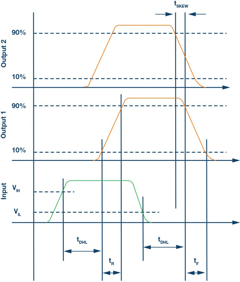
Decisive factors for minimizing switching times are output rise time (tR), fall time (tF), and the propagation delay (tD). The propagation delay is defined as the time needed for an input edge to reach the output and is dependent on the driver output current and the output load. The propagation delay usually behaves with minimal differences between the rising and falling edges, whereby a certain pulse width distortion (PWD) arises:

Because drivers often have multiple output channels, which have different response times despite being driven by the same input, a small, additional offset, the propagation delay skew (tSKEW), is yielded.
Click image to enlarge
Figure 3: Timing behavior of a gate driver with multiple outputs
Click image to enlarge
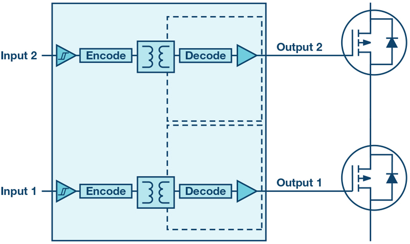
Figure 4: Simple schematic of a gate driver with multiple outputs
Insulation Withstand Voltage
In power electronics, insulation is needed for both functional and safety reasons. Because gate drivers are used, for example, in the form of a half-bridge topology in drive technology and thereby come in contact with high bus voltages and currents, insulation is unavoidable. The functional reason is that actuation of the power stage usually occurs from the low voltage circuit and hence actuation of the high-side switch of the half bridge would not be possible due to the higher potential with a simultaneously open low-side switch. At the same time, the insulation represents reliable isolation of the high voltage section from the control circuit in the event of a fault, so that contact by humans is possible. Insulated gate drivers typically exhibit dielectric strengths of 5kV (rms)/minor higher.
Immunity
Harsh industrial environments require the best possible immunity or interference resistance of the applications to sources of interference. For example, RF noise, common-mode transients, and magnetic interference fields are critical because they can couple into the gate driver, and can excite the power stage so that it switches at undesirable times. With insulated gate drivers, the common-mode transient immunity (CMTI) defines the ability for common mode transients between the input and the output to be rejected. For example, the ADuM4121 exhibits an excellent value of >150kV/µs.
The addressed parameters solely represent one part of the specifications for a gate driver and do not represent a complete list. Other decisive factors can include the operating voltage, the supply voltage, the temperature range, and additionally integrated functions such as a Miller clamp and desaturation protection. Thus, a large number of different gate drivers can be selected based on the requirements of the application.