Using SiC MOSFETs and packaging tech for next-gen systems
Current market requirements are trending towards further downsizing and increased efficiency of power conversion systems. For this reason, enhanced power density of the power modules will be critical in order to respond to the evolving needs of the market. In order to increase the power density, All-SiC modules with SiC-MOSFETs and SiC-SBDs are expected as one of the most powerful candidates for an alternative to Si modules. Here, All-SiC modules with the 1st generation trench gate SiC MOSFETs and new concept package are presented.
1st generation trench gate SiC MOSFETs
In order to achieve higher efficiency and size reductions for various power conversion systems, lower Ron is need. As is well known, shrinking of cell pitch is one means to increased channel density of SiC MOSFETs. However, the excessive shrinkage of cell pitch with planer gate MOSFET causes the increase of Junction Field-Effect Transistor (JFET) resistance.
From this point of view, applying trench gate MOS structure in place of planar gate is an effective method to avoid increasing JFET resistance by shrinkage of cell pitch. The developed 1st generation trench gate SiC MOSFETs have been optimized in terms of device parameter and process parameter. As a result, RonA of 3.5mΩcm2 for 1st generation trench gate SiC MOSFETs has been achieved.
Electrical performance of all-SiC Module
Electrical characteristics of 1200V/35A rated all-SiC module with 1st generation trench gate SiC MOSFETs and 7th generation Si module were compared. The evaluated all-SiC module is composed of 1st generation trench gate SiC MOSFET chip and SiC SBD chip in one leg, while the 7th generation Si module is composed of 7th generation IGBT chip and 7th generation FWD chip which were produced by Fuji Electric.
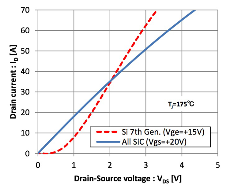
As shown in Figure 1, at 175˚C, the on-state voltage of all-SiC module was reduced under 35A of drain current ID in comparison with the 7th generation Si module. However, the current density of 1st generation trench gate SiC MOSFET chip at 35A of the rated current was around 1.6 times larger compared to 7th generation IGBT chip. This characteristic implies the reduction of steady loss because power modules installed in some equipment, in general, work at around half of the rating current. As shown in Figure 2, the forward voltage of all-SiC module was reduced in almost all the forward current area, compared to the 7th generation Si module.
Click image to enlarge
Fig. 1: Si 7th Gen./All-SiC output characteristic
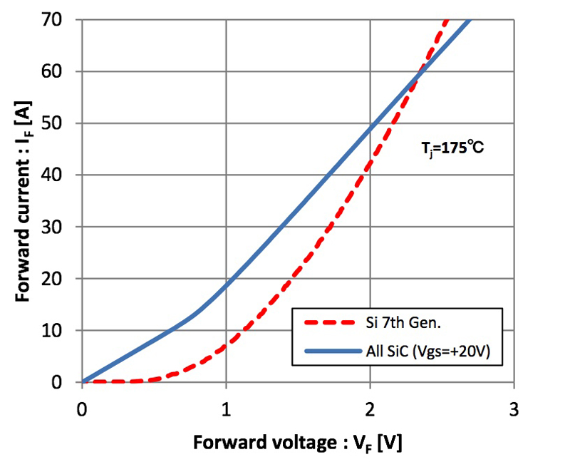
Fig. 2: Si 7th Gen./all-SiC 3rd quadrant characteristic
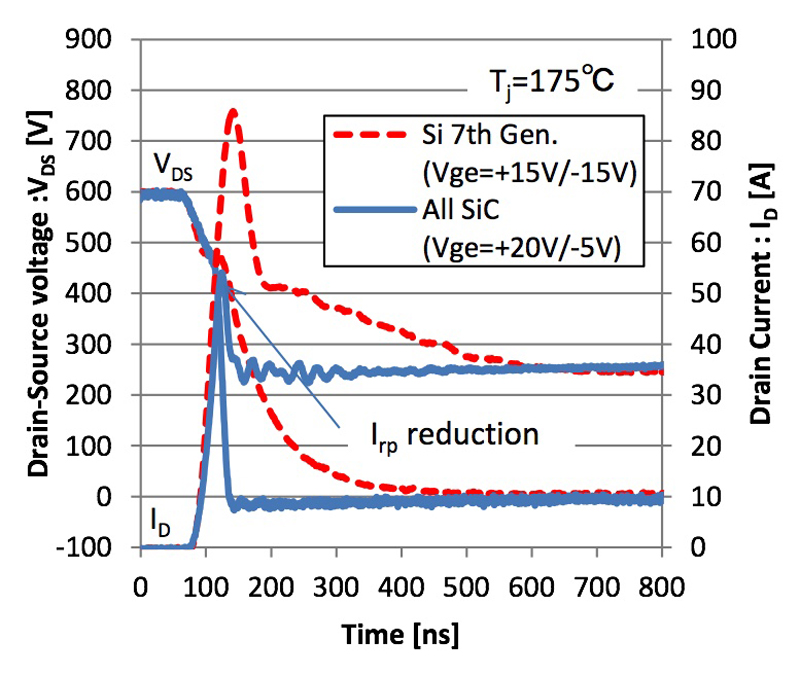
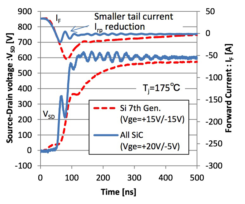
Dynamic characteristics of all-SiC module with 27Ω of the recommended gate resistance (Rg) and 7th generation Si module with 12Ω of the recommended Rg were compared. For the turn off waveforms, as shown in Figure 3 (a), the tail current of all-SiC module was reduced and the rising voltage was also faster compared to Si 7th generation IGBT module. Figure 3 (b) and (c) show the turn on and reverse recovery waveforms, respectively.
Click image to enlarge
Fig. 3: Switching waveforms (a) Turn-off waveforms (b) Turn-on waveforms (c) Reverse recovery waveforms

Click image to enlarge
Click image to enlarge
The peak current at turn-on of the all-SiC module was reduced compared to 7th generation Si IGBT module. This is because the peak current at reverse recovery (Irp) of the all-SiC module was reduced. In addition, as shown in Figure 3(c), the tail current of all-SiC module was reduced compared to the 7th generation Si IGBT module. These characteristics are caused by only majority carrier operation for the all-SiC module, while the minority carrier contributes to switching characteristics in the IGBT.
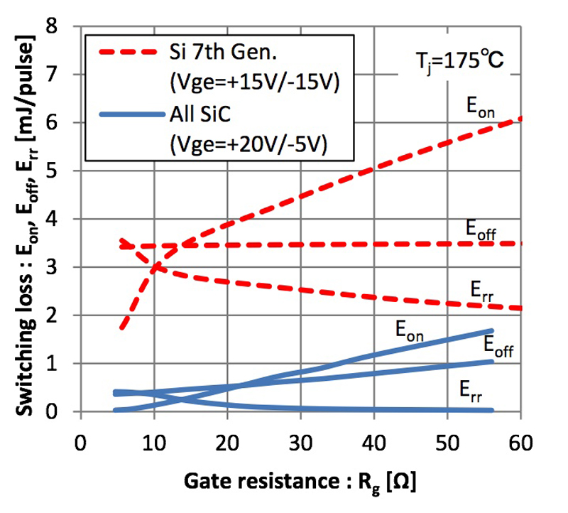
The switching losses depending on Rg were shown in Figure 4. Turn on loss (Eon) and turn off loss (Eoff) were increased monotonically with Rg, while reverse recovery loss (Err) was decreased monotonically with Rg. Switching losses between the all-SiC module with 27Ω of Rg and 7th generation Si IGBT module with 12Ω of Rg were compared. Eon, Eoff and Err for the all-SiC module was reduced by 77%, 82%, and 97%, respectively, as shown in Table 1. As a result, total switching loss (Esw_total) was dramatically reduced by 85% compared to the 7th generation Si module. Here, Esw_total means the sum of Eon, Eoff and Err. This result shows that reduction of switching loss for the inverter is expected.
Click image to enlarge
Fig. 4: Switching losses with a gate resistance
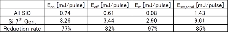
Table 1: Switching losses
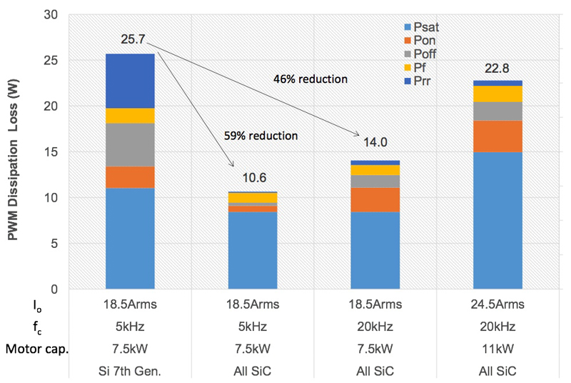
As shown in Figure 5, dissipation losses in PWM operation were simulated. Dissipation loss for the all-SiC module was greatly reduced by 59% compared to 7th generation Si IGBT module under conditions that Io is 18.5Arms and fc is 5 kHz. When the fc for all-SiC module was raised from 5 kHz to 20 kHz, the dissipation loss was reduced by 46% compared to 7th generation Si IGBT module.
Click image to enlarge
Fig. 5: Simulation of PWM dissipation loss
Furthermore, even when the Io for the all-SiC module was raised from 18.5Arms to 24.5Arms under conditions that fc is 20 kHz, the dissipation loss was almost the same compared to 7th generation Si IGBT module. These results can indicate that 1 rank extension for inverter capacity can be realized by applying all-SiC modules, even if fc during inverter operation is higher than IGBT.
For the reasons described above, all-SiC modules can contribute to the downsizing of the power conversion systems by miniaturization of filter from the effect for high fc operation and enhanced power density with 1 rank extension for inverter capacity.
All-SiC module with new concept package
The new concept package achieved low thermal impedance and high power density by thick copper block on the isolation substrate and a flexible board to conduct current. The thick copper block on the isolation substrate reduces thermal impedance of whole structure.
Furthermore, high thermal conductive SiN ceramic substrate is applied to isolation substrate.
The flexible board has copper pin connections between the flexible board and power chips, so there is no bonding Al wire. This pin connection structure contributes to reduce the package size of the module and lower internal inductance.
To realize high reliability, resin molding is the key to reduce thermal stress that accelerates fatigue-like damages in joining materials. Thus, high-Tg (Tg: glass-transition temperature) epoxy resin is applied to achieve endurance against high temperature operations. Generally, as Tg of resin increases, stability of thermal expansion is refined.
Joining materials play significant roles in determining the lifetime of the module since they directly receive thermal stress during operation. Material strength of the solder is expected to dominate the module lifetime because of its capability to withstand mechanical fatigue. In this point, low temperature melting solder has the limitation for high-temperature operations.
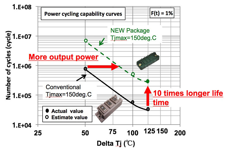
Considering the facts described above, joining material that is able to withstand high temperature and new composite resin are utilized to realize high reliability. As shown in Figure 6, compared to conventional modules, their refined joining structures with resin-molded packages have around 10 times longer lifetime in the condition of Tjmax = 150˚C and delta T = 125˚ Increase of product lifetime or more output power in a given operating condition are expected.
Click image to enlarge
Fig. 6: Reliability test delta Tj Power Cycle
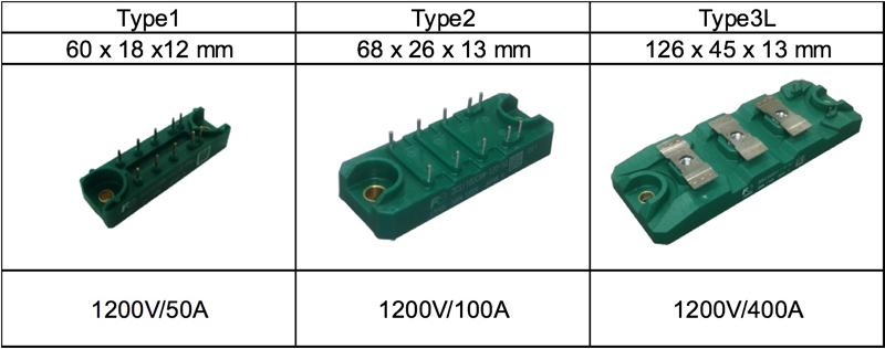
Figure 7 shows the lineup for the new concept package. The product lineup will realize coverage of the wide range inverter capacities in the market.
Click image to enlarge
Fig. 7: All-SiC line-up idea with 1st Gen.
Looking forward
All-SiC module with 1st generation trench gate SiC MOSFETs and new concept package have been introduced. The developed all-SiC module showed drastic low dissipation losses in the inverter loss simulation. These results may give us more power density and high frequency operation for all-SiC modules. We believe that all-SiC module with 1st generation trench gate SiC MOSFETs and new concept package will contribute greatly to the downsizing of power conversion systems in the future.