By improving the robustness and systematic capability of power supply blocks, related systematic failures can be eliminated
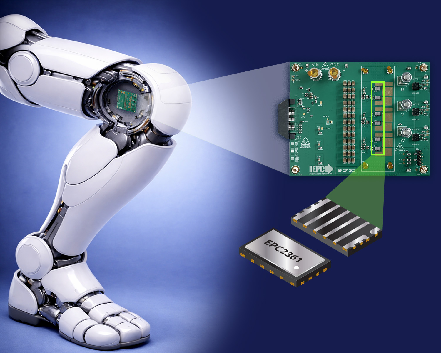
Figure 1: Example autonomous mobile robot (AMR) subsystems
Power supply blocks provide one of the most critical functionalities in electronics systems, as their behavior affects how the system will behave during the different modes of operation—power-up, power-down, steady-state operation, and in the event of failures—which is critical in achieving the safe state in functional safety applications. Note that one of the three key requirements in complying with the basic functional safety standard is systematic capability. This requirement focuses on preventing and controlling systematic failures, which arise from design flaws, errors in specification, and poor management processes. With such requirements comes the need to address systematic failures of a power supply.
Eliminating systematic failures due to a power supply involves using the correct specification, providing the necessarysequencing, and ensuring that their loads are always operating within their margins. Image sensors in sensor subsystems and microcontrollers in logic subsystems are one of the most sensitive components in a safety-related system, as shown in Figure 1. If system reset involves automatically restarting the power supply to such subsystems, it may incur damage to the components.
For an image sensor, having an incomplete power-up or power-down cycle stresses its circuitries.When the system is turned off, power to the image sensor should also be turned off as quickly as possible so the imager can be promptly restarted under ideal conditions, namely with no voltages lingering in the circuit. If the sensor is powered from a typical linear regulator, even though power to the regulator may turn off, the regulator’s output is often held up by the output capacitor, allowing the image sensor to remain powered up and potentially disrupting the desired turn-off and turn-on performance of the system.
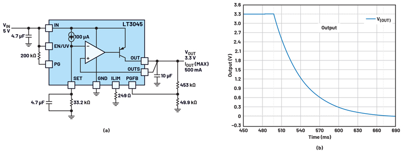
Figure 2 shows an example of a power supply with 3.3V on a 10µF output capacitor. This example has a 160ms discharge time into a 10kΩ load simulated using LTspice.
Click image to enlarge
Figure 2: Power supply example (a) using an LDO and (b) its output voltage discharge time
Using Output Discharge Functions
One way to ensure that output voltages are fully discharged upon turnoff is by using output discharge functions. These functions are necessary in applications requiring exact power sequencing and faster turn-off times, as they address floating outputs of power rails upon system power down to alleviate issues during power cycling.
Adding an External MOSFET as a Discharge Circuit
In recent power management designs, more low dropout (LDO) regulators are being released with additional functionality, including the increasingly common power-goodsignal (PGOOD). Such a PGOOD signal is a status output from the LDO, typically used to inform the system when the output voltage has reached and is maintaining proper regulation. In most implementations, this signal comes from an open-drain MOSFET that changes state based on the regulator’s status. When the LDO output is within regulation, the PGOOD MOSFET is turned off—resulting in high impedance at the pin and causing the PGOOD output pin to be pulled up high. However, when the output is out of regulation, the MOSFET turns on, pulling the PGOOD pin low via its low impedance path. This type of configuration allows the PGOOD signal to interface easily with different logic levels and supply voltages, making it versatile and widely usable.
However, this is also where a design challenge arises. Since the open-drain MOSFET used in most LDO PGOOD outputs is designed primarily for housekeeping, it can only sink a small amount of current. It is not suitable for sinking large currents directly from the output capacitor, especially if the goal is to quickly discharge the output when the LDO is disabled or shut down. Attempting to do so could damage the device or simply prove ineffective.
Click image to enlarge
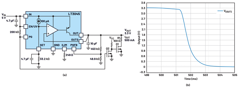
Figure 3: (a) Using the PGOOD signal of the LT3045 to trigger external MOSFETs as a discharge circuit and (b) its discharge time of 3.2ms at 10kΩ output load
A more robust solution utilizing the PGOOD signal is by combining it with an external MOSFET circuit, which will act as a controlled discharge path. As shown in Figure 3, this circuit uses a discharge resistor, R1, which determines how quickly the output capacitor will discharge. The designer can size this resistor based on the desired discharge time—larger resistors will discharge the capacitor more slowly, while smaller resistors will speed up the discharge time. In this configuration, MOSFET Q1 serves as the discharge switch that turns on when the converter is disabled through the enable pin (EN). Meanwhile, Q2 is responsible for inverting the logic of the PGOOD signal from the LDO, ensuring the correct timing of Q1’s activation. This setup allows for a fully customizable active discharge circuit that is responsive to the LDO’s status.
By employing this method, any LDO equipped with a PGOOD pin can effectively be upgraded with an external active output discharge feature. This offers great flexibility for designers, allowing them to fine-tune the discharge profile of their power rail. The trade-off, however, is the added cost and board space due to the external components. Nevertheless, in applications where precise discharge control is critical, this approach provides a valuable and customizable solution.
Implementing an Integrated Solution
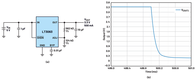
To address this need without external circuitry, Analog Devices offers LDO solutions with integrated active discharge functionality. For instance, the LT3063 features a built-in active output discharge mechanism that simplifies the design process, reduces component count, and saves PCB space while still providing quick discharge performance. Figure 4 shows using this device achieves a discharge time of 0.5ms, a significant improvement over the previous example in Figure 3.
Click image to enlarge
Figure 4: (a) LT3063 example circuit and (b) its discharge time of 0.5ms at 10kΩ output load
Using a Supervisory Circuit
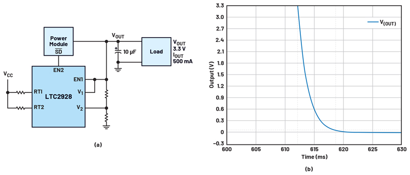
In safety-critical applications, a separate supervisory circuit may be preferred to provide more reliability and a sufficient degree of independence. A power supply sequencer such as the LTC2928 integrates the overvoltage and undervoltage monitoring features required to comply with functional safety, power sequencing, and output discharge capability. Figure 5 shows an example circuit. Other supervisory circuits with the output discharge feature include the MAX16050 and MAX16051.
Click image to enlarge
Figure 5: (a) LT2928 example circuit and (b) its discharge time of 6.5ms at 10kΩ load
Conclusion
Selecting the appropriate approach to address a power supply output’s discharge performance requires a thorough evaluation of the design requirements and operating conditions. The methods for implementing active output discharge have their own distinct advantages and trade-offs. A certain solution may be more effective under specific output or application scenarios, while another method could offer better performance in different conditions. Therefore, understanding the unique characteristics and limitations of each technique is essential to ensure optimal implementation.
An external MOSFET is typically preferred in applications that demand higher output voltages or where maximum flexibility is needed. However, designers must be willing to accept the trade-offs of higher cost, increased board space, and additional power loss due to the inverter circuit. However, integrated solutions are often the best choice for low power or space-constrained designs, as they require no extra components and avoid further power dissipation. The drawback is limited availability, since only certain LDOs provide this feature. Furthermore, supervisory circuits are well-suited for systems with multiple output rails where power sequencing is also important. Although their MOSFET sink current is limited, making them less effective for large output capacitors, they provide an excellent option when sequencing, system coordination, and a degree of independence for functional safety consideration are critical. In summary, the decision should be based on matching the method’s strengths to the specific output voltage, space, required discharge time, and sequencing requirements of the application.