Infineon Reaches Next Milestone on 200 mm Silicon Carbide Roadmap: Product-Roll out to Customers Starts
Infineon releases first silicon carbide products to customers based on advanced 200 mm SiC wafer manufacturing technology
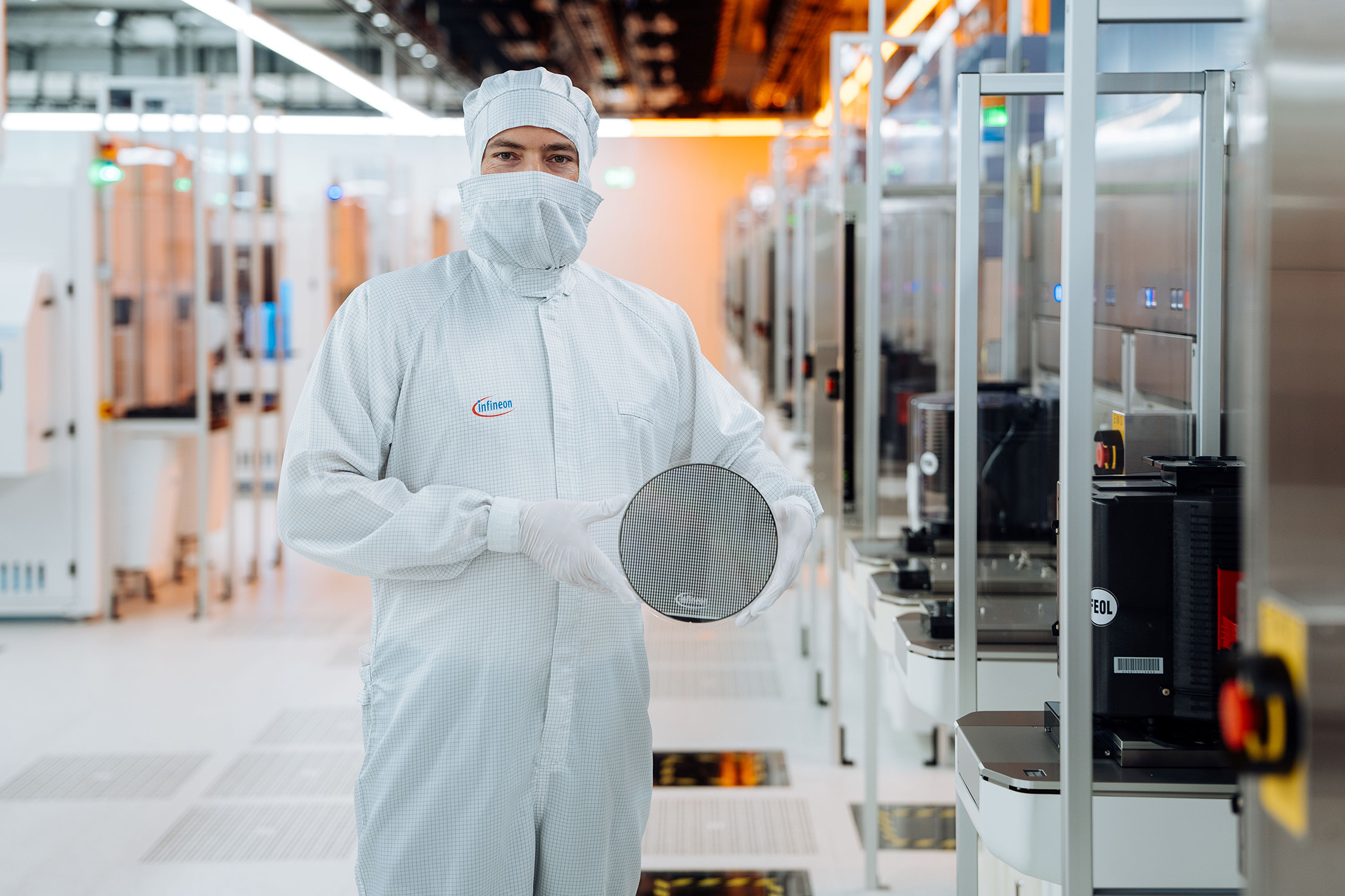
Infineon Technologies AG has made significant progress on its 200 mm silicon carbide (SiC) roadmap. The company will already release the first products based on the advanced 200 mm SiC technology to customers in Q1 2025. The products, manufactured in Villach, Austria, provide first-class SiC power technology for high-voltage applications, including renewable energies, trains, and electric vehicles. Additionally, the transition of Infineon's manufacturing site in Kulim, Malaysia, from 150-millimeter wafers to the larger and more efficient 200-millimeter diameter wafers is fully on track. The newly built Module 3 is poised to commence high-volume production aligned with market demand.
“The implementation of our SiC production is progressing as planned and we are proud of the first product releases to customers,” said Dr. Rutger Wijburg, Chief Operations Officer of Infineon. “By ramping up SiC production in Villach and Kulim in phases, we are improving cost-efficiency and continuing to ensure product quality. At the same time, we are making sure our manufacturing capacities can meet the demand for SiC-based power semiconductors.”
SiC semiconductors have revolutionized high-power applications by switching electricity even more efficiently, demonstrating high reliability and robustness under extreme conditions, and by making even smaller designs possible. Infineon’s SiC products let customers develop energy-efficient solutions for electric vehicles, fast charging stations and trains as well as renewable energy systems and AI data centers. The release to customers of the first SiC products based on the 200-millimeter wafer technology marks a substantial step forward in Infineon’s SiC roadmap, with a strong focus on providing customers with a comprehensive portfolio of high-performance power semiconductors that promote green energy and contribute to CO 2 reduction.
As “Infineon One Virtual Fab” for highly innovative wide-bandgap (WBG) technologies, Infineon’s production sites in Villach and Kulim share technologies and processes which allow for fast ramping and smooth and highly efficient operations in SiC and gallium nitride (GaN) manufacturing. The 200-millimeter SiC manufacturing activities now add to Infineon’s strong track record of delivering industry-leading semiconductor technology and power system solutions and strengthen the company’s technology leadership across the entire spectrum of power semiconductors, in silicon as well as in SiC and GaN.