Implementing Efficient Isolation in Digital Power Supplies
The challenge of isolation in a digital power supply is in sending digital or analog signals across the isolation barrier with fast speed, accuracy, and compact size.
However, the traditional optocoupler solution has low bandwidth and current transfer ratio (CTR), which causes wide variation with temperature and degradation with time problems. The transformer solution also has bulk size, magnetic saturation problems, etc. These issues limit optocoupler or transformer use in some high reliability, compact size, and long life applications.
Why You Need Isolation
When designing a power supply, complying with safety standards is essential to protect operators and other personnel from electric shock and hazardous energy. Isolation is an important method to meet safety standards. The isolation requirement specifies different levels of input and output voltage—both steady state and transient state—by many agencies throughout the world like VDE and IEC in Europe and UL in the United States. For instance, there are five categories of insulation introduced in UL60950:
· Functional Insulation: Insulation that is only necessary for the correct functioning of the equipment.
· Basic Insulation: Insulation to provide basic protection against electric shock
· Supplementary Insulation: Independent insulation applied in addition to basic insulation, in order to reduce the risk of electric shock in the event of a failure of the basic insulation.
· Double Insulation: Insulation that comprises both basic insulation and supplementary insulation.
· Reinforced Insulation: A single insulation system that provides a degree of protection against electric shock and is equivalent to double insulation under the conditions specified in this standard.
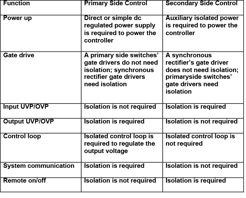
Primary Side Control and Secondary Side Control Comparison
According to the position of the controller, the isolated power control methods divide into two types: primary side control and secondary side control. Table 1 shows the function comparison between the primary side control and secondary side control. UVP and OVP stand for undervoltage protection and overvoltage protection, respectively, in the below table.
Table 1. Function Comparison Between the Primary Side Control and Secondary Side Control
Secondary Side Control
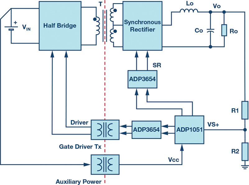
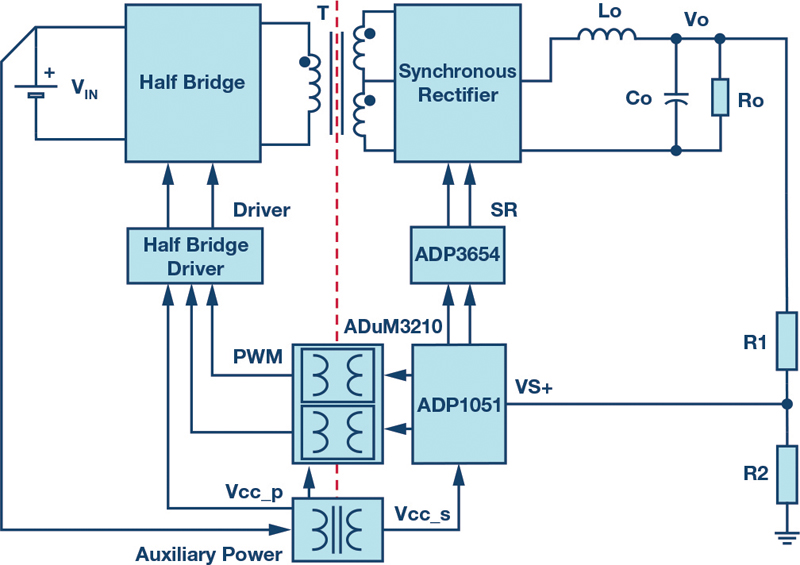
The ADP1051 is an Analog Devices’ advanced digital power controller with a PMBus interface, which targets high power density and high efficiency applications like intermediate bus converters.[1] The ADP1051 is based on flexible state machine architecture and provides many attractive features such as reverse current protection, prebias startup, constant current mode, adjustable output voltage slew rate, adaptive dead time control, and volt-second balance inside the chip, which reduces lots of external components compared with analog solution. Generally, the ADP1051 is used more often as secondary side control, as it is easy to have it communicate with the system. Therefore, signals such as PWM signals of synchronous rectifiers and VOUT sensing do not need to cross the isolation boundary to communicate with the system. However, in this case, an auxiliary power supply is required to provide the initial power to the secondary side controller ADP1051 at the start up stage from the primary side. In addition, PWM signals, which are from ADP1051, need to cross the isolation boundary. Three approaches are discussed, which are gate drive transformer, digital isolator, and isolated gate driver.
Gate Drive Transformer
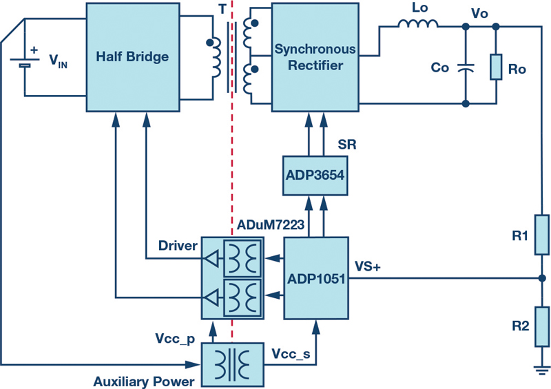
Figure 1 shows the block diagram of a digital power supply with the gate drive transformer solution. In this approach, the secondary controller ADP1051 sends PWM signals to the ADP3654, which is a dual-channel, 4 A MOSFET driver. The ADP3654 then drives a gate drive transformer. The function of gate drive transformer is to transfer the drive signals from the secondary side to the primary side, and drive the primary side MOSFETs. An auxiliary isolated power supply provides the power to ADP1051 at start up stage.
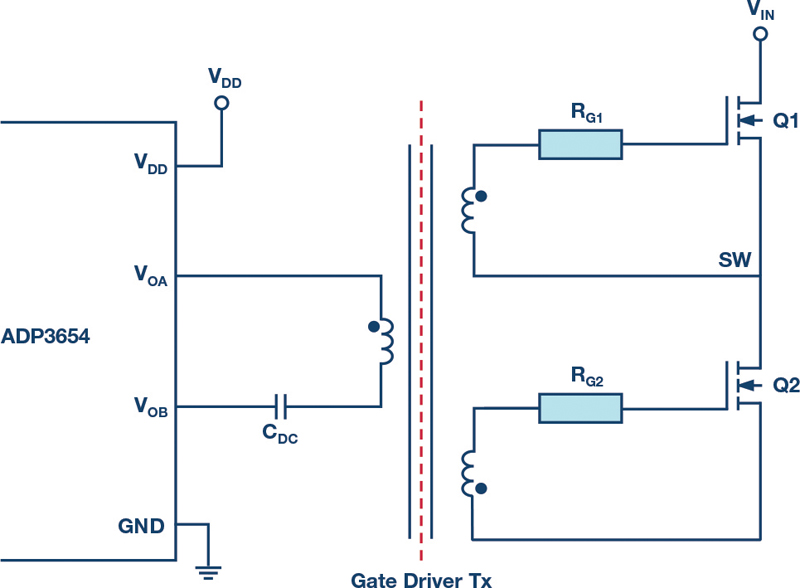
The advantages of the gate drive transformer solution include minor time delay and lower cost. However, ADP3654 requires more careful design of the gate drive transformer, as the transformer needs to be reset after a period of on time—otherwise, it will saturate. In terms of gate drive transformer design for a half bridge topology, a double-ended transformer often is employed, which is shown in Figure 2.
Figure 2 shows the circuit of a gate drive transformer driven by the ADP3654. The ADP3654s VOA and VOB outputs connect to a gate drive transformer through a dc blocking capacitor CDC. Considering the maximum volt seconds required under all operating conditions, a maximum 50% duty cycle is selected for half bridge. Once the core is selected, the number of primary winding NP can be calculated by using Equation 1:
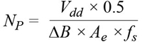
Where VDD is the voltage across the primary winding, fs is the switching frequency, ΔB is the peak-to-peak flux density change during half of the switching period, and Ae is the equivalent cross section area of the core. When VOA drives high and VOB drives low, Q1 is turned on and Q2 is turned off. When VOB drives high and VOA drives low, Q2 is turned on and Q1 is turned off. Note that this gate drive transformer is suitable for symmetrical half bridge, but not for asymmetrical half bridge or other active clamp topology.
Click image to enlarge
Figure 2. Double-ended gate drive transformer
Digital Isolator
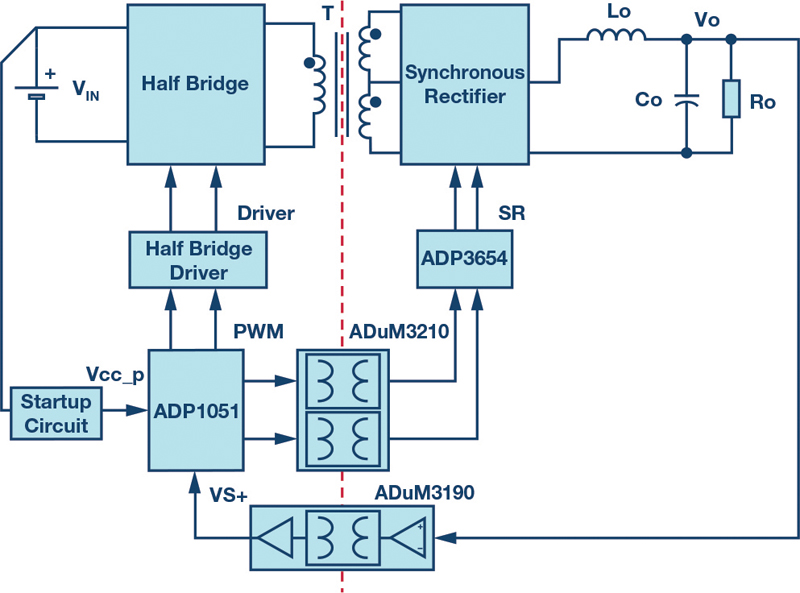
Figure 3shows a block diagram of a digital power supply, which implements a digital isolator solution. The dual-channel digital isolator ADuM3210 is used as digital isolation to transfer the PWM signals from the secondary side controller ADP1051 to the primary side half bridge driver.
Click image to enlarge
Figure 3. Digital isolator solution
Compared to the complex gate drive transformer design, the digital isolator solution is smaller, more reliable, and simpler to use. There is no limitation to the duty cycle and this solution does not have the saturation issue. Because it saves over 50% PCB space, this solution can achieve a high power density design.
Isolated Gate Driver
To further simplify the design, integrated electrical isolation, and strong gate drive capability, the ADuM7223, 4 A, isolated half bridge gate driver can provide independent and isolated high-side and low-side outputs. The isolated gate driver solution is shown in Figure 4.
Click image to enlarge
Figure 4. Isolated gate driver solution
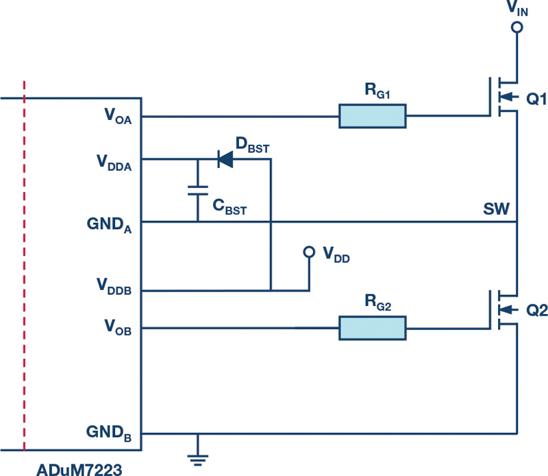
In Figure 5, the ADuM7223 isolated gate driver is configured as a bootstrap gate driver to drive a half bridge. DBST is an external bootstrap diode and CBST is an external bootstrap capacitor. During each cycle when the low side MOSFET Q2 turns on, VDD charges the bootstrap capacitor through the bootstrap diode. To minimize the power dissipation, a low forward voltage drop and fast reverse recovery time, ultrafast diode is required.
Click image to enlarge
Figure 5. Isolated gate driver configured as a bootstrap gate drive
Primary Side Control
Because primary side control does not need an auxiliary isolated power supply and has a simple control architecture, utilizing primary side control is more popular in some low cost applications. According to the isolating control path, three approaches are discussed: linear optocoupler, general optocoupler with standard amplifier, and isolated amplifier.
Linear Optocoupler
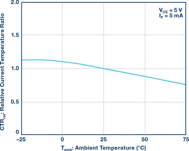
Isolating the output voltage in a digital power supply generally requires fast and accurate isolating feedback. The optocouplers are often used to send analog signals from the secondary side to the primary side, but the CTR of the optocoupler varies in a very wide range with temperature, and it degrades with time. Figure 6 shows the normalized CTR vs. ambient temperature characteristic of TCET1100. From this figure, the variation of CTR will exceed 30% from –25°C to +75°C.
Click image to enlarge
Figure 6. Normalized CTR vs. temperature of TECT1100
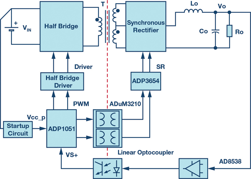
It is very hard to guarantee the output voltage accuracy with a general optocoupler used directly in the feedback loop to transfer the output voltage. A general optocoupler is used with an error amplifier to transfer the compensation signal instead of the output voltage. The ADP1051 already has the digital loop compensation implemented inside of the chip, so it does not need the compensation signal anymore. One way around this is to use a linear optocoupler solution to transfer the output voltage linearly, as shown in Figure 7. The cost of a linear optocoupler is high, which means the user has to pay a premium.
Click image to enlarge
Figure 7. Linear optocoupler solution
General Optocoupler with Standard Amplifier
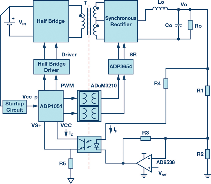
Another circuit can be applied to realize primary side control using a general optocoupler and a standard amplifier, which is shown in Figure 8. In this case, high output voltage accuracy is achieved without suffering from the wide CTR range of the optocoupler due to temperature changes. The measurement results show the output voltage variation is in the range of ±1%, with the CTR range from 100% to 200%.
Click image to enlarge
Figure 8. Optocoupler with amplifier solution
The formula of CTR is

When CTR changes with temperature, the output of the amplifier will compensate the changes to maintain high accuracy on the output voltage. Note that the stable operation point and the swing range of the amplifier should be well designed to satisfy the CTR variation with the temperature requirement, in case the output of the amplifier saturates.
Isolated Amplifier
The third method is the isolated amplifier, like the ADuM3190, which is shown in Figure 9. The ADuM3190 is an isolated amplifier that is ideal for linear feedback power supplies with primary side controllers, due to its high bandwidth and high accuracy compared to an optocoupler. This enables improvements in transient response, power density, and stability, as compared to commonly used optocoupler and shunt regulator solutions. With the proper design, the ADuM3190 can achieve ±1% output voltage accuracy.
Click image to enlarge
Figure 9. Isolated amplifier solution