This article looks at high-side GaN FET gate measurements taken with advanced isolated probes compared to alternative equipment and techniques
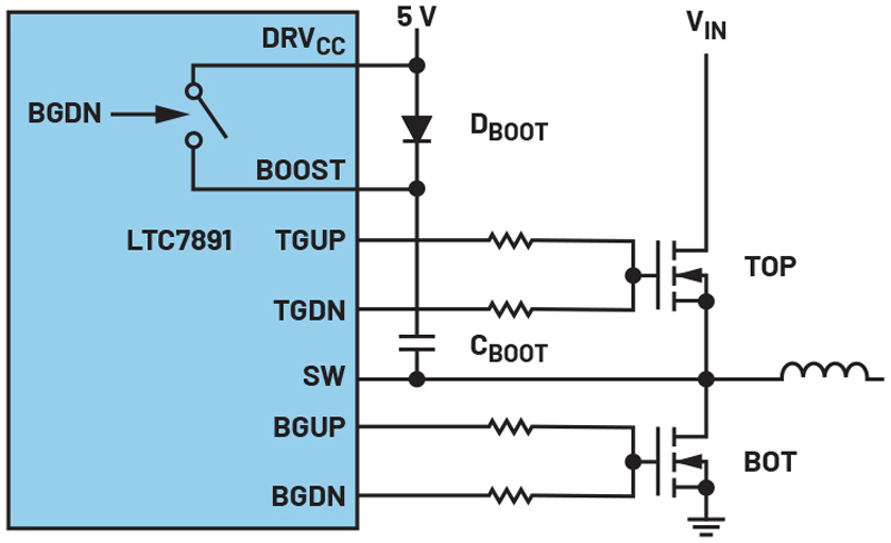
Figure 1: The LTC7891 step-down (buck) converter schematic
Gallium nitride field-effect transistors (GaN FETs) offer faster switching speeds, smaller packages, and lower power losses than silicon FETs. These features allow power converters to run at higher frequencies, reducing overall solution size while maintaining high efficiency. While the basic DC-to-DC converter design remains the same, GaN introduces additional design and testing challenges. One of the more important challenges is precise control of gate voltage and timing. This can be difficult because the switching times can exceed what traditional controllers and test equipment can manage. Fortunately, GaN-specific controllers and measurement techniques can solve these problems and ensure a reliable power supply design without adding extra complexity.
GaN Performance and Characteristics
Figure 1 shows a 12V step-down converter based on the LTC7891 synchronous controller driving 100 V GaN FETs. Operating at 500 kHz, it achieves 97% efficiency with a 20 A load and 48 V input. This is about 2% higher efficiency — 40% less power loss — than with current generation 100 V silicon FETs. * To match this performance with silicon, the switching frequency would need to be less than half, requiring a larger inductor and overall solution size. This device is part of the new family of controllers specifically designed to meet GaN’s gate drive and switching requirements without the need for additional components. Analog Devices’ portfolio of GaN-optimized controllers also includes the LTC7890, a 100V dual-channel buck controller, along with the LTC7893 and LTC7892, which serve as 100V boost and dual-channel boost controllers, respectively.
* The LTC7891 controller features 4V to 5.5V gate drive suitable for GaN and logic level silicon FETs. The LTC7897 controller, with 5V to 10V gate drive, is suitable for standard level silicon FETs.
Gate Voltage
Silicon FETs are typically specified with a gate-source voltage between 4.5V and 10V and an absolute maximum rating of ±20V. In contrast, a 100V GaN FET might be specified with a gate-source voltage of 5 V limited to +6 V/-4 V for long-term reliability. Meeting these GaN specifications requires a tightly regulated gate supply and minimal high frequency overshootor undershoot. While a precise 5 V supply is sufficient for the low-side FET, additional circuitry or a GaN-specific controller is needed to limit the high-side FET’s gate-source voltage.
Gate Driver Supply
In Figure 2, a bootstrap capacitor and diode (CBOOT and DBOOT) implement a traditional high-side gate drive supply. When the high-side (TOP) switch turns off, the switch node pulls low — either due to the inductor current or the low-side (BOT) switch turning on. With both switches off, the switch node’s voltage is limited to approximately 1 V below ground by the silicon FET’s bodydiode. In contrast, GaN FETs conduct in the reverse direction,performing like a 2 V to 3 V body diode. When using a bootstrap diode, the negative switch voltage adds to the bootstrap capacitor’s voltage, increasing the high-side FET’s gate-source voltage. Alternatively, a smart switch can prevent the driver from overcharging without the need for extra clamping diodes. This active switch turns on after the BOT gate is on, resulting in a regulated high-side gate drive voltage that does not depend on the body diode drop. In the case of extended dead times, these controllers tolerate negative spikes on the switch node. With a stable high-side driver supply established, the next step is accurately measuring the high-side FET’s gate-source voltage.
Click image to enlarge
Figure 2: GaN controller with internal smart bootstrap switch
Gate Measurements
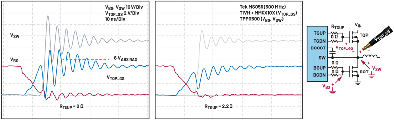
Figure 3 shows the gate and switch waveforms of a GaN-based step-down (buck) converter. Without a series gate turn-on resistor, the TOPFET’s gate-source voltage (VTOP_GS) exceeds the GaN FET’s specified +6 V maximum gate-source voltage rating. Adding a 2.2 Ω TGUP resistor reduces VTOP_GS and dampens gate and switch node ringing. High impedance oscilloscope probes capture the ground-referenced low-side gate (VBG) and switch node (VSW) waveforms. The TOP FET’s source (VSW) alternates between VIN and ground. The GaN’s high slew rate (over 30 V/ns) and 300MHz ringing exceed the practical common-mode limit of differential probes typically used to make VTOP_GS measurements. Fortunately, available optically isolated probes make this measurement possible. These probes, pioneered by Tektronix’s IsoVu technology, feature unbelievably high frequency common-mode rejection ratio (CMRR) and are priced accordingly.
Click image to enlarge
Figure 3: Turn-on wave forms with isolated probe
Isolated probes connect to the oscilloscope through fiber optic cables, which not only provides galvanic isolation but also keeps common-mode input capacitance low. The probe’s attenuator tip plugs directly into an MMCX connector. The probe can also connect to PCB test points using header pins and an MMCX-to-square-pin adapter. To maintain the probe’s full performance, the connection between the probe tip and the PCB is kept as short and well-shielded as possible. A board-mounted MMCX connector offers the best coaxial connection, but make sure to route short Kelvin traces from the FET gate and source. While the isolated probe may be the best—and only—way to measure high-side GaN gate voltages, let’s see how another common method stacks up.
Passive Probes
High-side gate signals can be measured with two ground-referenced passive probes, a digital oscilloscope, and math. This A − B or pseudo differential technique remains popular for evaluating gate timing on low-voltage DC-to-DC converters, even though it suffers from limited voltage range and CMRR. Before taking high-side gate measurements, it’s best to do a quick common-mode rejection check. Connect both the probes to the same high dv/dt voltage, deskew the timing, subtract one channel from the other, and observe the remaining signal. If the CMRR is adequate, only a small residual voltage should be seen—much less than the actual gate signal. Probe loading is another key factor. Ideally, probing should not affect circuit operation or waveforms. Standard high impedance passive probes have an input impedance of 10 MΩ in parallel with 3.9 pF to 10 pF.
In contrast, isolated probes have a lower capacitance (under 2pF) to ground. There are also less common, low-impedance (500Ω to5 kΩ) passive probes** that offer low capacitance, which can be helpful in these measurements.
Results
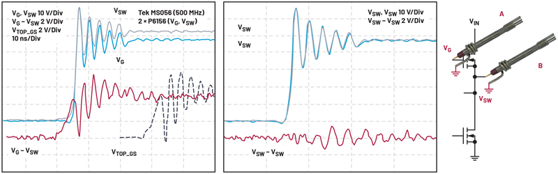
Figure 4 compares the VG–VSW waveform, captured using the A – B method, to the VTOP_GS measurement from the earlier Figure 3 isolated probe setup (shown as a dashed line). For this test, low impedance passive probes (5 kΩ // < 2 pF) were selected because higher capacitance probes (≥3.9 pF) caused a noticeable decrease in VSW’s peak amplitude, indicating probe loading. The gate waveforms are a reasonable match, though the A–B method shows a 2.7V peak-to-peak residual common-mode signal—high compared to the 7 V peak-to-peak VG – VSWsignal. High impedance passive probes showed similar levels ofresidual common-mode noise, but the measured VG – VSW peakswere 17% to 30% lower, likely due to loading, matching, and response issues.
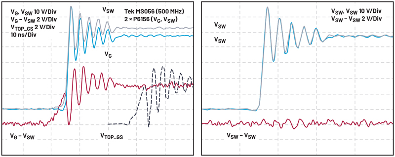
In Figure 5, VG and VSW were captured using a single passive probe in two steps. With this method, the VG waveform is captured and saved in memory. The same probe is then moved and used to capture VSW. Note that a second probe, connected to VSW, triggers the oscilloscope during both measurements. Channel math is used to recall and subtract the waveforms. This approach adds an extra step but improves common-mode rejection by avoiding probe mismatches. While high impedance passive probes performed better than expected, the low impedance probes provided results that more closely matched those of the trusted isolated probe, making them the preferred choice in this case.
Click image to enlarge
Figure 4: TOPFET gate measurement (VG–VSW) using A–B method
Click image to enlarge
Figure 5: TOPFET gate measurement (VG-VSW) using one probe
** Referred to as high frequency, low impedance resistor divider, 50 Ω or Z0 probes.
Conclusion
Low voltage GaN DC-to-DC converters offer clear size and performance advantage over their silicon counterparts. However, these benefits come with new challenges, including the need for precise gate voltage control and accurate high-side gate measurements. With the right combination of GaN-optimized controllers and appropriate measurement techniques, these challenges can be addressed—enabling robust, efficient designs without the need for additional circuitry.