LPDDR6 Bandwidth Math: What You Gain, What You Pay, What You Measure

A practical look at how Low-Power Double Data Rate 6 (LPDDR6) increases bandwidth with less energy, and why validation matters more than ever
Figure 1: LPDDR6 expands beyond mobile. Conventional LPDDR apps (phone, client, IoT, automotive, XR) extending into AI data center, Smart NIC, robotics, and high-performance laptops
There is an old engineering adage that a system is only as fast as its slowest component, and AI systems are no different. As models scale, one of the first bottlenecks to surface is memory.
Because of the importance of memory, Joint Electron Device Engineering Council (JEDEC) LPDDR6 is positioned as a next-generation low-power memory standard designed to push per-pin data rates beyond 10.6 Gbps while targeting meaningful reductions in active and standby power, up to ~30% versus the prior generation. Because it improves performance per watt, LPDDR6 is expected to find applications well beyond mobile, including AI and ML platforms, high-speed digital systems, automotive, edge deployments, smart NICs, robotics, and high-performance laptops where thermal limits are real.
What You Gain: Bandwidth and a wider path for AI-era data movement
One of the biggest design choices with LPDDR6 was how to handle the increase in throughput. Options include increasing the data clock speed (faster clocks), increasing the number of bits per sample (multi-level), increasing the channel width (wider channels), and increasing efficiency (burst length).
Faster clocks
Speed-wise, LPDDR6 is expected to scale up to 14.4 Gbps. It is a solid jump from LPDDR5X's ~9.6 Gbps cap. But the real story isn't just the raw clock speed.

Click image to enlarge
Figure 2: JEDEC LPDDR timeline. Generational rise in MT/s (mega-transfers/sec) per pin (data rate per DQ)
Simpler Signaling
Instead of making the jump to PAM4 signaling (multi-level), the designers of LPDDR6 stayed with traditional two-level NRZ. This keeps voltage margins wide and receiver designs relatively simple. To get that extra bandwidth, they instead choose a wider interface.
Wider Channels for AI-era Data Movement
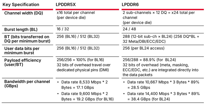
Beyond raw speed, LPDDR6 introduces a fundamental change to its channel architecture. While LPDDR5 utilized a 16-bit channel width, LPDDR6 moves to a 24-bit width, composed of two 12-bit sub-channels.
This redesign also cleans up the physical layout. With LPDDR5 and 5X, you had to duplicate pins like Clock (CK) and Chip Select (CS) for every single channel. LPDDR6 fixes this by letting sub-channels share a single CK pair and other non-command signals, like RESET. A smart way to cut down on total pin count and make motherboard routing easier.
Burst Length and Effective Bandwidth
To maximize these speed gains, LPDDR6 introduces a new Burst Length of 24 (BL24), a step up from the BL16 standard in LPDDR5. By combining these higher data rates with the wider 24-bit channel, LPDDR6 is expected to deliver:
· Initial targets: 28.5 GBps effective bandwidth.
· Defined: Up to 38.4 GBps (at 14.4 Gbps), doubling the performance of LPDDR5X-9600.
What You Pay: Efficiency overhead & protocol complexity
One trade for simplifying the interface is removing dedicated pins; as a result, some of what moves on the bus is no longer pure payload. LPDDR6 also introduces additional operating voltages and behaviors that shape the real performance per watt.
Fewer sideband pins, more “inside the data”
As we touched on earlier, LPDDR6 eliminates a lot of extra sideband pins by including their information directly into the main data stream. LPDDR5 uses dedicated pins, such as DMI, solely for Data Masking and Inversion. LPDDR6 drops those entirely, packing all that metadata straight into the data transfer itself. Considering the PCB trace densities in current designs, the change provides some relief for anyone designing a motherboard, as it simplifies routing. Still, it also makes the protocol more complex and adds overhead you have to plan for.
Let's look at the math: during a BL24 access, the system moves 288 bits in total. You get 256 bits of actual user data, and the remaining 32 bits handle the overhead (including masking, ECC, and EDC). That leaves LPDDR6 with an 88.9% payload efficiency. Still, it's probably a worthwhile trade-off for a much cleaner physical layout and a more robust system.
Click image to enlarge
Figure 3: LPDDR6 performance targets. >10 Gbps per pin, 24-bit channels (2x12), ~28.5 GB/s initially, up to ~38.4 GB/s at 14.4 Gbps
Power: dual-rail Dynamic Voltage and Frequency Scaling (DVFS) and smarter I/O energy per bit
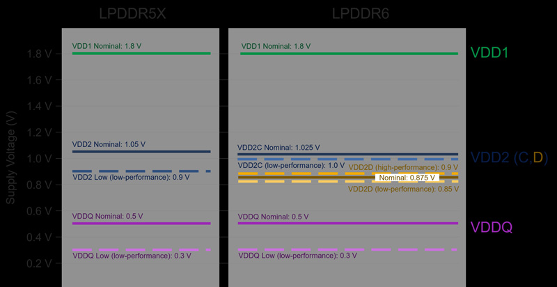
Since power consumption is proportional to supply Voltage, it is not a surprise that LPDDR has been steadily reducing the core voltage, lowering it from around 1.8V to closer to 1.0V, and LPDDR5/5X introduced split VDD2 rails (VDD2H/VDD2L) to enable lower-voltage operation at lower speeds. LPDDR6 extends this approach with a dual-rail scheme (often described as VDD2C ~1.0 V and VDD2D ~0.875 V) to target ~20–30% lower operating power than LPDDR5X, further reducing energy consumption.
Click image to enlarge
Figure 4: LPDDR5X ®LPDDR6 rails & DVFS. Moves from VDD2H/VDD2L to dual rails (~1.0 V/ ~0.875 V) with more Dynamic Voltage Frequency Scaling (DVFS) operating performance points for lower operating power
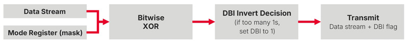
Enhanced Write Data Bus Inversion (DBI)
Data Bus Inversion (DBI) reduces power consumption by keeping more zeros than ones in the data stream. The host periodically computes optimal exclusive OR (XOR) masks based on observed traffic and inverts the data, since transmitting a 0 typically draws less power than a 1.
This approach to DBI may take a few additional operations, but it makes the system better at adapting to different data streams, including different AI models.
Click image to enlarge
Figure 5: Enhanced Write DBI. Host computes optimal XOR masks, store on mode registers, and inverts/encodes write data to reduce switching/termination power
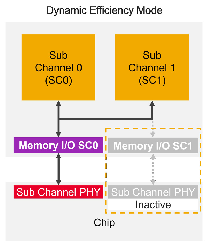
Power Dependent Dynamic Efficiency Mode
LPDDR6 also supports Dynamic Efficiency Mode. Here, the host can reduce SDRAM power at the expense of bandwidth by operating with only one sub-channel’s I/O while still accessing data across both sub-channels. Fewer switching and terminated I/O lines reduce dynamic toggle power and driver/termination current. It is a deliberate tradeoff lever: if the system is power-limited in a given operating state, it can give up peak bandwidth to stay within the envelope.
Click image to enlarge
Figure 6: Dynamic Efficiency Mode. One sub-channel I/O can access both, cutting I/O activity and power, with up to ~1/2 bandwidth trade off
What You Measure: Reliability and the validation burden at speed
At the end of the day, these design trade-offs only matter if designers and engineers can actually measure and repeat them in real silicon. With LPDDR6 pushing the limits of speed and power efficiency, reliability becomes part of the performance story, and validation needs to prove margin, fault behavior, and long-run robustness, not just peak bandwidth.
Reliability
LPDDR6 introduces a new signal, ALERT, which provides a mechanism for LPDDR6 devices to signal faults to the host. The ALERT pin will be High-Z when inactive, so that multiple device ALERT outputs can be connected to a single host input. The device can register up to 15 different faults via four Fault Registers. Faults such as Write ECC/EDC errors can be masked or reported in real time.
Advancing LPDDR6 Validation (Going Beyond Physical Pins)
As LPDDR6 pushes per-pin data rates toward 14.4 Gbps, the transition from theoretical simulation to hardware validation presents new engineering challenges. In addition, with dedicated DMI pins removed, LPDDR6 carries additional data within DQ — simplifying routing and reducing pin count but increasing the complexity of signal integrity analysis. To address this, the industry has evolved its validation workflow to bridge the gap between pre-silicon design and physical testing:
- Pre-Silicon Design: Engineers increasingly model LPDDR6 channel and package configurations. This allows for early evaluation of link performance and potential signal loss before physical hardware is fabricated.
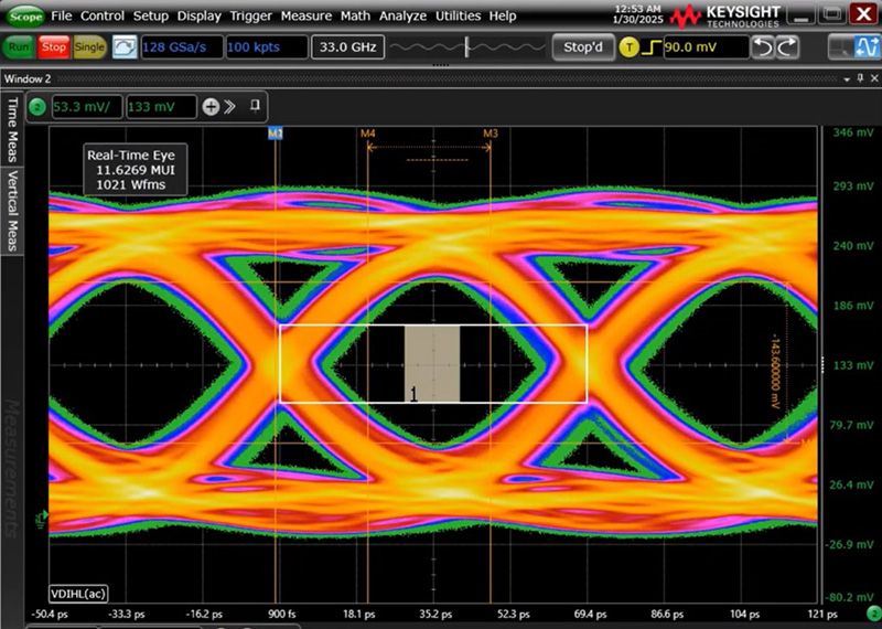
- Extrapolated Eye-Mask Requirements: Another evolution in the LPDDR6 specification is the transition to extrapolated eye-mask testing. Unlike previous generations that focused on timing and signal-quality measurements like slew rate and setup/hold timing, LPDDR6 requires an eye-mask analysis extrapolated to a Bit Error Rate (BER) of 1E-16. This ensures long-term reliability in high-speed AI and edge computing environments.
- Read/Write Data Timing - WCK & RDQS vs DQ Precision: Increased focus on Validation of the critical timing relationship between the Read/Write Clocks and the Data (DQ) signals. Using advanced compliance software and high-bandwidth oscilloscopes, designers can verify margins and ensure signal integrity at the extreme speeds required for LPDDR6.
Click image to enlarge
Figure 7: LPDDR6 transmitter compliance results. Real-time eye diagram captured on a Keysight UXR oscilloscope showing eye opening and compliance mask
Conclusion
LPDDR6 is not just a faster LPDDR. It's designed to resolve several memory challenges that emerge as AI scales: bandwidth per watt, tighter signal margins, and reliability under real workloads. As new memory technologies like LPDDR6, HBM4, and GDDR7 come to market, testing becomes more demanding. The constant design and validation challenge is finding ways to reduce time-to-market without cutting corners on accuracy. Starting with design tools that simulate the entire system upfront and make all relevant measurements (eye margin, BER, timing, and skew analysis), making it much easier to catch timing and skew issues early, such as Keysight ADS Memory Designer. On the measurement side, designers and engineers need to look for memory workflows that make this easier by covering the entire process from start to finish, such as the Keysight portfolio, including automated transmitter testing, intensive receiver stress testing, and probes specifically designed for these unforgiving signals.