Author:
Molly Zhu, and Fei Guo, Analog Devices
Date
05/03/2021
 PDF
PDF
Click image to enlarge
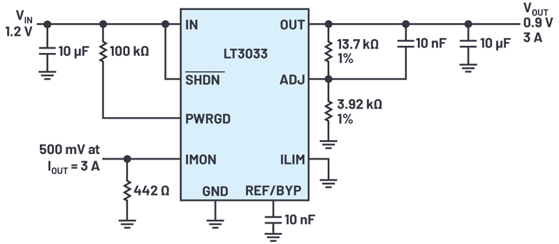
Figure 1. LT3033 typical application
Each successive generation of computing systems demands more total power and lower supply voltages than its predecessor, challenging power supply designers to keep pace with higher output current in a small area. At high power densities with low output voltages, the problem of heat dissipation rises to the top of the design priority list, especially for linear regulators in low noise applications. Paralleling LDO regulators can increase the supply current capability and mitigate heat dissipation, reducing the temperature rise of any particular component and the required size and number of coolingdevices.
This article shows how to parallel the 3 A LT3033 very low dropout regulator (VLDO) for applications that require a current higher than 3 A, with the added benefit of spreading heat dissipation. The LT3033 can be easilyparalleled—and current balanced—due to its built-in output current monitoring feature.
The LT3033 converts 1.14 V to 10 V input supplies to outputs as low as 0.2 V with load currents up to 3 A. The dropout voltage is only 95 mV at full load. Quiescent current is 1.8mA during operation, dropping to 22µA when shut down. Programmable current limit and thermal protection give it the necessary robustness for high-current, low-voltage applications.
3 A single VLDO application
Figure 1 shows the LT3033 delivering 0.9 V at 3 A from a 1.2 V input supply. A minimum of 10µF very low ESR ceramic capacitor is required at the IN and OUT pins for stability. Adding a feedforward capacitor (CFF) from VOUT to the ADJ pin can improve the transient response and lower the output voltage noise. A 10 nF bypass capacitor from the REF/BYP pin to GND typically reduces output voltage noise to 60µV rms in a 10Hz to 100kHz bandwidth and soft starts the reference. The minimum input voltage required for regulation equals the regulated output voltage VOUT plus the dropout voltage or 1.14 V, whichever is greater. A demonstration board is shown in Figure 2.

Click image to enlarge
Figure 2. LT3033 demonstration board
Current limit is programmable by connecting a single resistor from the ILIM pin to GND, accurate to ±12% over a wide temperature range. The external current limit may be overridden by internal current limit with foldback when the input and output differential voltage exceeds 5 V.
LT3033 provides an output current monitor by pulling the IMON pin to GND through a resistor. The IMON pin is the collector of a PNP, which mirrors the LT3033 output PNP at a ratio of 1:2650. The resistor voltage is proportional to the output current if it is not higher than VOUT – 400mV.

This output current monitor enables current sharing for multiple LT3033s.
Despite its tiny size, the LT3033 also includes a number of protection features, including internal current limit with foldback, thermal limit, reverse current, and reverse-battery protections.
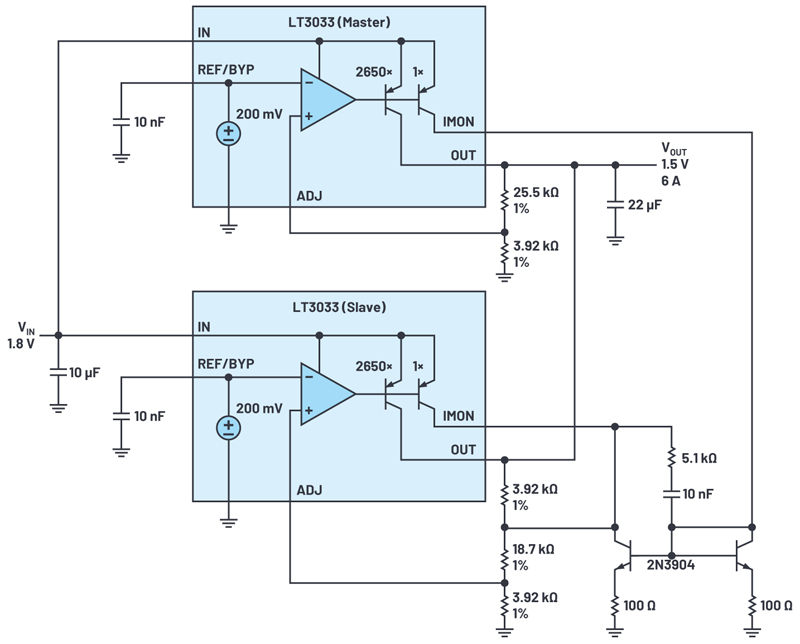
Two LT3033s in parallel in a 6 A application
For applications that require more than 3 A, multiple LT3033s can be paralleled by taking advantage of its current monitor feature. Figure 3 illustrates two LT3033s in parallel together with two 2N3904 NPN devices to generate a 1.5 V, 6 A output. The individual IN pins and OUT pins are tied together, respectively. One LT3033 acts as master, controlling the LT3033 slave device.
Click image to enlarge
Figure 3. Paralleling two LT3033s
The IMON pins combined with an NPN current mirror create a simple amplifier. This amplifier injects current into the feedback divider of the slave LT3033 to force the IMON currents from each LT3033 to be equal. The 100 Ω resistors provide 113 mV emitter degeneration at full load to guarantee good current mirror matching. The output voltage of the slave LT3033 is set at 1.35 V, 10% lower than the circuit output to ensure the master LT3033 stays in control. The feedback resistors of the slave LT3033 are split into sections to ensure adequate headroom for the slave NPN. A 10 nF, 5.1 kΩ capacitor and resistor combination added to the IMON pin of the slave device frequency compensates the feedback loop.
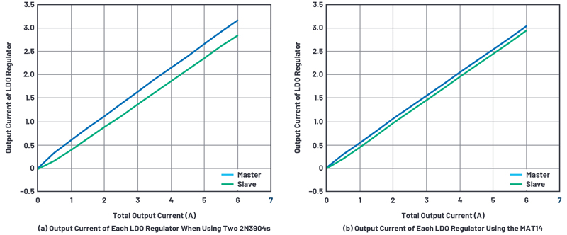
Though this circuit can supply 6A load current, current sharing accuracy is limited by the mismatch between two NPN devices—mismatches result in uneven heat distribution on the board. Higher current sharing accuracy can be achieved by using a matched monolithic transistor, such as the MAT14 from Analog Devices, to replace the two discrete NPN devices. The MAT14 is a quad monolithic NPN transistor that offers excellent parametric matching. Its maximum current gain matching is 4%.
Figure 4 compares the output current of each LDO regulator using discrete and matched NPN devices, respectively. Compared to the 2N3904, the MAT14 current mirror reduces the current mismatch from 5.3% to 1.6 %.
Click image to enlarge
Figure 4. Current sharing mismatch is reduced by using the MAT14 matched monolithic quad transistor with parallel LDO regulators
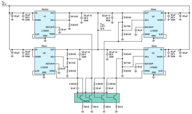
Paralleling four LT3033s
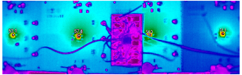
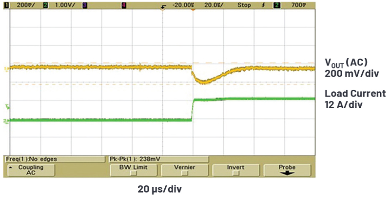
The paralleling circuit architecture is scalable to as many LT3033s as needed by extending the current mirror and adding slave LT3033 devices. Figure 5 shows a solution with four LT3033s in parallel using the MAT14 for current sharing. The thermal performance is shown in Figure 6. The four LT3033s reach temperatures ranging from 51°C to 58°C. Considering the voltage drop along the input trace for each part, the heat spreads evenly on the board, indicating balanced current sharing for this solution. Figure 7 shows the transient response of a 1.5 V output, 12 A power supply operating from a 1.8 V input.
Click image to enlarge
Figure 5. Four LT3033s in parallel using the MAT14
Click image to enlarge
Figure 6. Thermal performance of four LT3033s in parallel
Click image to enlarge
Figure 7. Load transient response of four LT3033s in parallel
Conclusion
The LT3033 is a 3 A VLDO regulator in a 3 mm × 4 mm package. Multiple LT3033 VLDO regulators can be paralleled for high current applications because of their built-in output current monitor feature. With only 95 mV typical voltage drop at full load, LT3033 is ideal for low input voltage to low output voltage, high current applications, yielding comparable electrical efficiency to a switching regulator. Other features include programmable current limit, power goodflag, and thermal limiting for reliable and robust solutions. Battery-powered systems benefit from low quiescent current and reverse-battery protection.