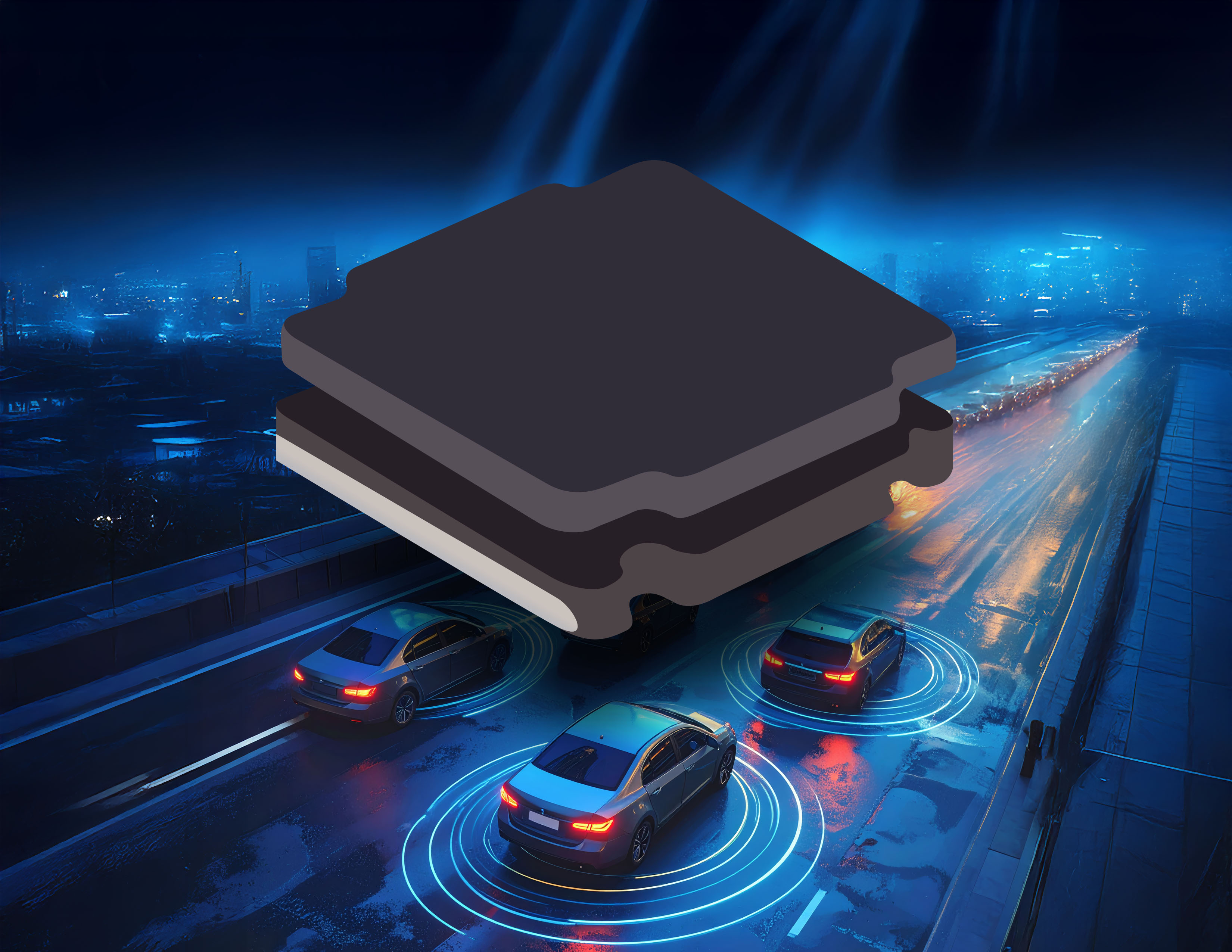
Next-generation devices empower advanced RF systems
As the overall size of communications, medical, and other cloud-enabled equipment continues to decrease, power management becomes an increasingly important design consideration. The latest highly-integrated power management solutions provide advantages in powering RF systems, FPGAs, and processors, and powerful design tools to help empower engineers to quickly implement a new design.
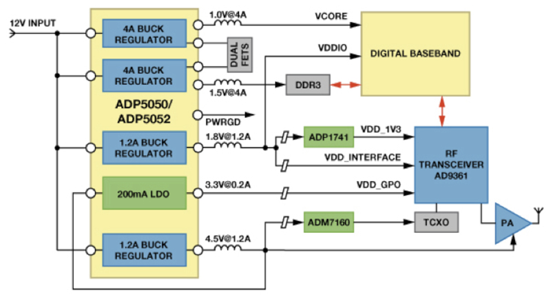
The emergence of femtocells and picocells in communications infrastructure is driving the need for smaller base stations, which have complex requirements for powering digital baseband, memory, RF transceivers, and power amplifiers in the smallest area with the highest power efficiency, as shown in Figure 1. A typical small cell system needs a very dense power supply that can deliver large currents with fast transient response to power the digital baseband, along with low-noise, low-dropout regulators (LDOs) to power the AD9361 RF Agile Transceiver, temperature compensated crystal oscillator (TCXO), and other noise-critical rails.
Click image to enlarge
Figure 1. Small base stations require a variety of power supplies
Setting the switching frequency of the switching regulators outside of the critical RF bands reduces noise, and synchronizing the switching regulators ensures that beat frequencies do not affect the RF performance. Reducing the core voltage (VCORE) of the digital baseband minimizes power consumption for low-power modes, and supply sequencing ensures that the digital baseband processor is up and running before the RF transceiver is enabled. An I2C interface between the digital baseband and the power management allows the output voltages of the buck regulators to be changed. To increase reliability, the power management system can monitor its own input voltage and die temperature, reporting any faults to the baseband processor.
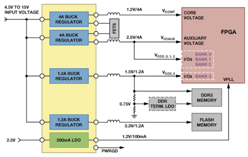
Similarly, the trend in medical and instrumentation devices—for example, portable ultrasound and handheld instrumentation—is toward significantly smaller form factors, so these products are driving the need for smaller, more efficient ways of powering FPGAs, processors, and memory, as shown in Figure 2. A typical FPGA and memory design needs a very dense power supply that can deliver large currents with fast transient response to power the core and I/O rails, along with a low-noise rail to power on-chip analog circuitry such as a phase-locked loop (PLL).
Click image to enlarge
Figure 2. Powering an FPGA-based system
Power supply sequencing is critical to ensure that the FPGA is up and running before the memory is enabled. Regulators with a precision enable input and a dedicated power-good output allows power supply sequencing and fault monitoring. Power supply designers often want to use the same power IC in different applications, so the ability to change the current limits is important. This design reuse can significantly reduce time to market—a critical element in any new product development process.
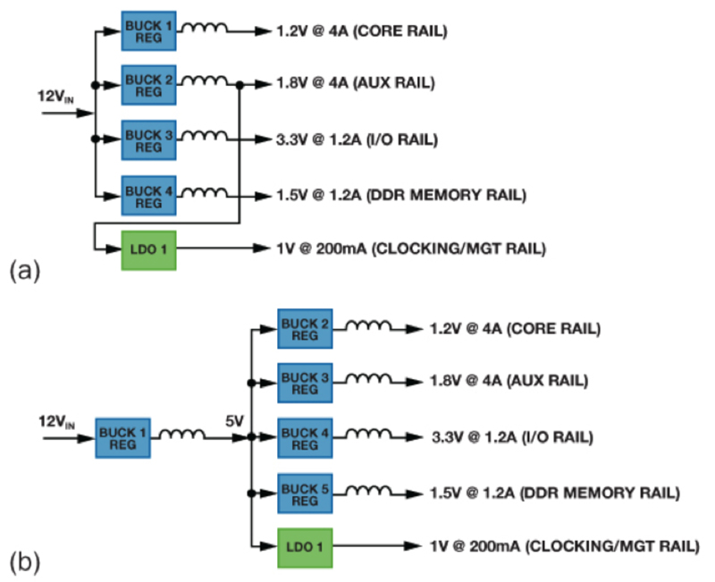
Consider a common multirail power management design specification for an FPGA with a 12-V input and five outputs:
• Core: 1.2 V @ 4 A
• Auxiliary: 1.8 V @ 4 A
• I/O: 3.3 V @ 1.2 A
• DDR memory: 1.5 V @ 1.2 A
• Clock: 1.0 V @ 200 mA
A typical discrete implementation, shown in Figure 3a, connects four switching regulators to the 12-V input rail. The output of one switching regulator pre-regulates the LDO to reduce power dissipation. An alternative approach, shown in Figure 3b, uses one regulator to step the 12-V input down to a 5-V intermediate rail, which is then regulated down to produce each of the required voltages. This implementation has a lower solution cost, but also a lower efficiency due to the two-stage power conversion. In both cases, each regulator has to be enabled independently, so supply sequencing may require a dedicated power supply sequencer. Noise may also be an issue, unless all of the switchers can be synchronized to reduce beat frequencies.
Click image to enlarge
Figure 3. (a) Discrete regulator design and (b) alternative discrete regulator design
Integrated solution yields high efficiency, small size
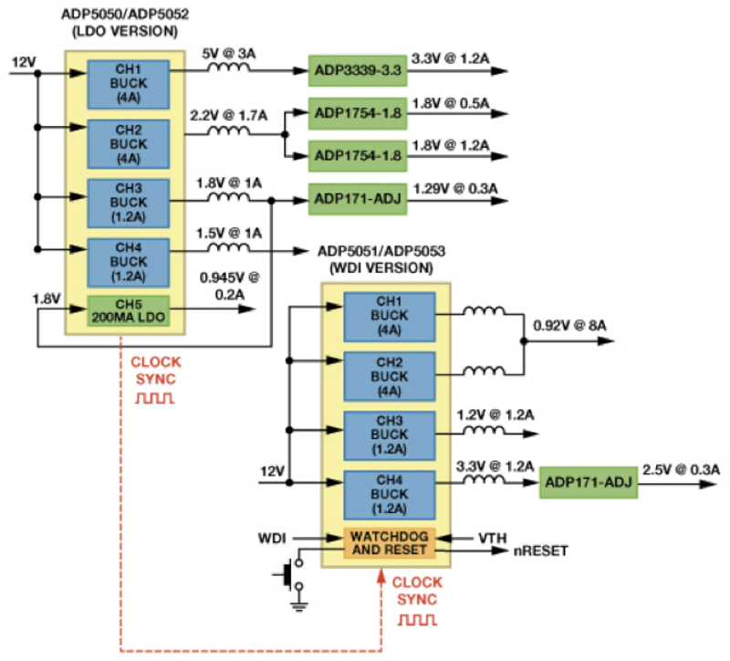
Integrating multiple buck regulators and LDOs into a single package can significantly reduce the overall size of a power management design. In addition, smart integrated solutions provide many advantages over traditional discrete implementations. Reducing the number of discrete components can significantly reduce the cost, complexity, and manufacturing cost of the design. The ADP5050 and ADP5052 integrated power management units (PMUs) can implement all these voltages and features in a single IC, using significantly less PCB area and fewer components.
For highest efficiency, each of the buck regulators can be powered directly from 12 V (similar to Figure 3a), removing the need for a preregulator stage. Buck 1 and Buck 2 have programmable current limits (4 A, 2.5 A, or 1.2 A), allowing the power supply designer to quickly and easily change the currents for new designs and significantly reducing the development time. The LDO can be powered from a 1.7-V to 5.5-V supply. In this example, the 1.8-V output from one of the buck regulators powers the LDO to provide a low-noise 1-V rail for the noise-sensitive analog circuitry.
The switching frequency, fSW, is set between 250 kHz and 1.4 MHz by resistor RRT. The flexible switching frequency range allows the power supply designer to optimize the design, reducing the frequency for highest efficiency or increasing the frequency for smallest overall size.
In some designs it is desirable to have both: a lower switching frequency to provide the highest power efficiency for the higher current rails, and a higher switching frequency to reduce inductor size and minimize PCB area for the lower current rails. A divide-by-two option on the master switching frequency allows the ADP5050 to operate at two frequencies, as shown in Figure 4. The switching frequency for Buck 1 and Buck 3 can be set via the I2C port to one-half of the master switching frequency.
Click image to enlarge
Figure 4. The ADP5050 operates at a low switching frequency for high efficiency on high-current rails and a high frequency for small inductor size on low-current rails
Power Supply Sequencing
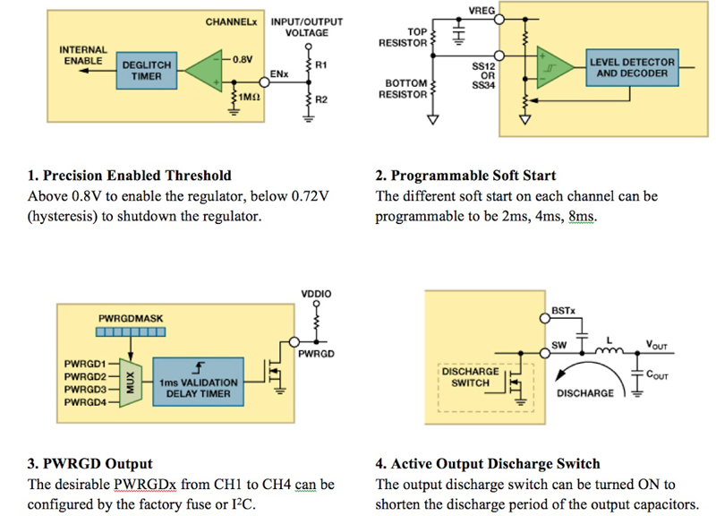
As shown in Figure 5, the ADP5050 and ADP5052 have four features that simplify power supply sequencing that is required for applications using FPGAs and processors: precision enable inputs, programmable soft start, a power-good output, and an active output discharge switch.
Click image to enlarge
Figure 5. ADP5050 and ADP5052 simplify power supply sequencing.
Precision Enable Inputs
Each regulator, including the LDO, has an enable input with a precise 0.8-V reference (Figure 5-1). When the voltage at an enable input is greater than 0.8 V, the regulator is enabled; when the voltage falls below 0.725 V, the regulator is disabled. An internal 1-MΩ pull-down resistor prevents errors if the pin is left floating. The precision enable threshold voltage allows easy sequencing within the device, as well as with external supplies. As an example, if Buck 1 is set to 5 V, a resistor divider can be used to set an accurate 4.0-V trip point to enable Buck 2, and so on, setting an accurate power-up sequence for all outputs.
Programmable Soft Start
Soft start circuitry ramps the output voltage in a controlled manner, limiting the inrush current. The soft start time is set to 2 ms when the soft start pins are tied to VREG, or it can be increased up to 8 ms by connecting a resistor divider from the soft start pin to VREG and ground (Figure 5-2). This configuration may be required to accommodate a specific start-up sequence or an application with a large output capacitor. The configurability and flexibility of the soft start enable large, complex FPGAs and processors to power up in a safe, controlled manner.
Power-Good Output
An open-drain power-good output (PWRGD) goes high when the selected buck regulators are operating normally (Figure 5-3). The power-good pins allow the power supply to signal the host system about its health. By default, PWRGD monitors the output voltage on Buck 1, but other channels can be custom ordered to control the PWRGD pin.
The status of each channel (PWRGx bit) can be read back via the I2C interface on the ADP5050. A logic high on the PWRGx bit indicates that the regulated output voltage is above 90.5% of its nominal output. The PWRGx bit is set to logic low when the regulated output voltage falls below 87.2% of its nominal output for more than 50 µs. The PWRGD output is the logical AND of the internal unmasked PWRGx signals. An internal PWRGx signal must be high for at least 1 ms before PWRGD goes high; if any PWRGx signal fails, PWRGD goes low with no delay. The channels that control PWRGD (Channel 1 to Channel 4) are specified by factory fuse or by setting bits via the I2C interface.
Active Output Discharge Switch
Each buck regulator integrates a discharge switch from the switching node to ground (Figure 5-4). Turned on when its associated regulator is disabled, the switch helps the output capacitor to discharge quickly. The typical resistance of the discharge switch is 250 Ω for Channel 1 to Channel 4. The active discharge switch pulls the output to ground when the regulator is disabled, even when a large capacitive load is present. This significantly increases the robustness of the system, particularly when it is power cycled.
I2C Interface
The I2C interface enables advanced monitoring capability and basic dynamic voltage scaling of the two buck regulator outputs (Channel 1 and Channel 4).
Input Voltage Monitor: The input voltage can be monitored for faults such as undervoltage conditions. As an example, with 12 V applied to the input, the I2C interface is configured to trigger an alert if the input voltage falls below 10.2 V. The signal on a dedicated pin (nINT) tells the system processor that a problem has occurred and shuts the system down for corrective action. The ability to monitor the input voltage increases system reliability.
Junction Temperature Monitor
The junction temperature can be monitored for faults such as overtemperature conditions. If the junction temperature increases above a preset level (105°C, 115°C, or 125°C), an alert is signaled on nINT. Unlike thermal shutdown, this function sends a warning signal, but does not shut down the device. The ability to monitor the junction temperature and alert the system processor to possible systems failures before they happen increases the system reliability.
Dynamic Voltage Scaling
Dynamic voltage scaling allows the system to reduce power consumption by dynamically lowering the power supply voltage on Channel 1 and Channel 4 for low-power modes, or it can dynamically change the output voltage depending on the system configuration and system loading. Also, the output voltages of all four buck regulators can be set via the I2C interface.
Low Noise Features
Several features reduce system noise generated by the power supply:
Wide Resistor Programmable Switching Frequency Range: A resistor on the RT pin programs the switching frequency between 250 kHz and 1.4 MHz. This flexibility allows the power supply designer to set the switching frequency to avoid system noise bands.
Buck Regulator Phase Shifting
The phase shift of the buck regulators can be programmed via the I2C interface. By default, the phase shift between Channel 1 and Channel 2 and between Channel 3 and Channel 4 is 180°. The benefit of out-of-phase operation is reduced input ripple current and less ground noise on the power supply.
The phase shift of Channel 2, Channel 3, and Channel 4 can be set to 0°, 90°, 180°, or 270° with respect to Channel 1 using the I2C interface. When parallel operation is configured to provide a single combined output of up to 8 A on Channel 1 and Channel 2, the switching frequency of Channel 2 is locked to a 180˚ phase shift with respect to Channel 1.
Clock Synchronization
The switching frequency can be synchronized to an external clock in the 250-kHz to 1.4-MHz range via the SYNC/MODE pin. This ability is important in RF and noise-sensitive applications. When an external clock is detected, the switching frequency transitions smoothly to its frequency. When the external clock stops, the device switches back to the internal clock and continues to operate normally. Synchronizing to an external clock allows the system designer to stay away from critical noise frequency bands and reduces the noise generated by multiple devices in a system.
For successful synchronization, the internal switching frequency must be programmed to a value close to that of the external clock value; a frequency difference of less than ±15% is suggested.
The SYNC/MODE pin can be configured as a synchronization clock output via a factory fuse or the I2C interface. A positive clock pulse with a 50% duty cycle is generated at the SYNC/MODE pin with a frequency equal to the internal switching frequency. A short time delay (~15% of tSW) occurs between the generated synchronization clock and the Channel 1 switching node.
Figure 6 shows two devices configured in frequency synchronization mode: one device is configured as the clock output to synchronize the other device. A 100 kΩ pull-up resistor should be used to prevent logic errors if the SYNC/MODE pin is left floating. Both devices are synchronized to the same clock, so the phase shift between Channel 1 of the first device and Channel 1 of the second device is 0°.
Clcik image to enlarge
Figure 6. RF application shows two devices synchronized to reduce power supply noise.
ADIsimPower Design Tool
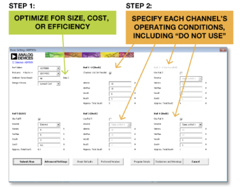
ADIsimPower now supports the ADP5050/ADP5052 multichannel high-voltage PMUs, which power 4/5 channels with load current up to 4 A per channel from inputs up to 15 V. The design tool allows users to optimize the design by cascading channels, placing high-current channels in parallel to create an 8-A rail, and considering the thermal contributions of each channel. With the advanced features, users can independently specify each channel’s performance for ripple and transient performance, switching frequency, and channels that support half the master frequency.
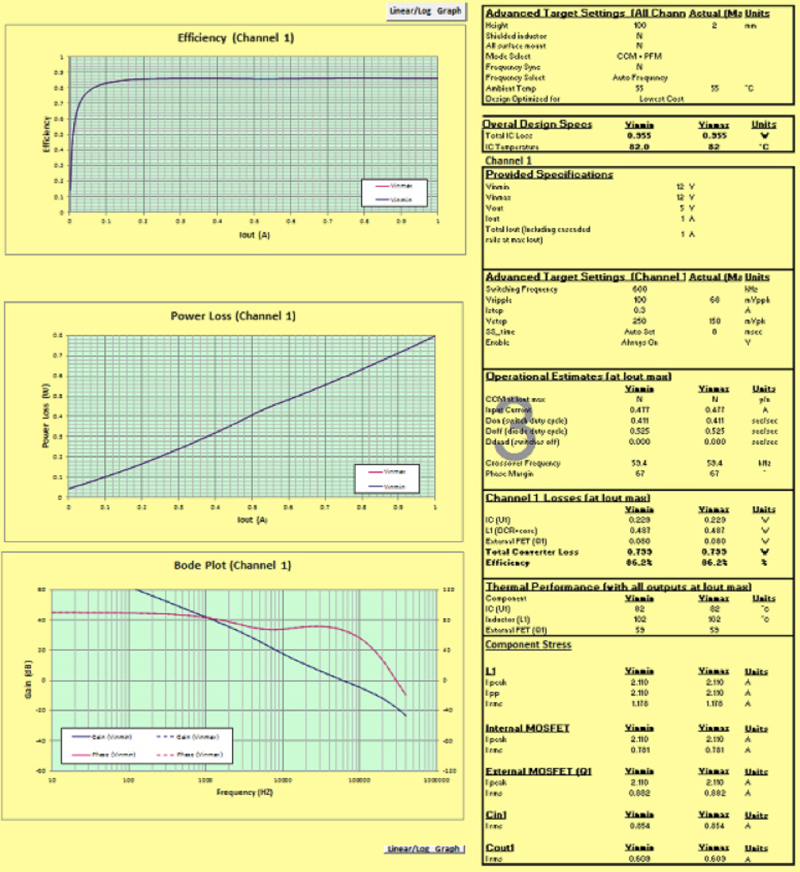
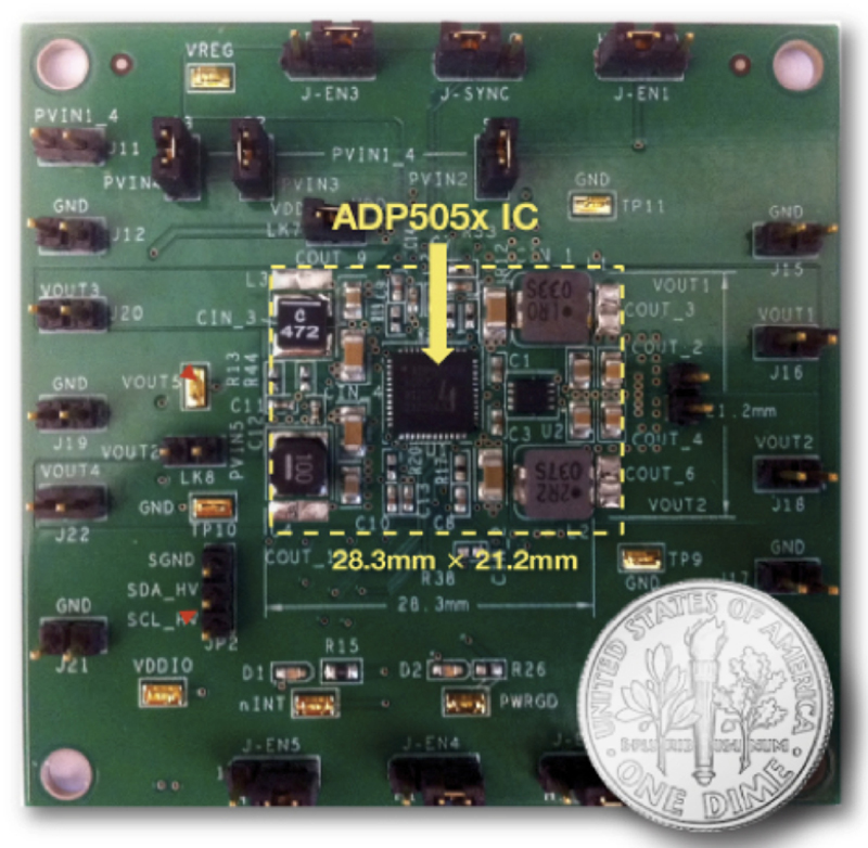
ADIsimPower allows the user to quickly and easily input the design requirements on the software interface shown in Figure 7. A full bill of materials is generated with intelligent component selection. Evaluation boards can be requested from within the tool. ADIsimPower gives the power designer quick access to accurate, tested, reliable performance data, as shown in Figure 8. The design can then be assembled on an evaluation board, as shown in Figure 9.
Click image to enlarge
Figure 7. ADIsimPower software interface.
Click image to enlarge
Figure 8. ADIsimPower simulation output.
Click image to enlarge
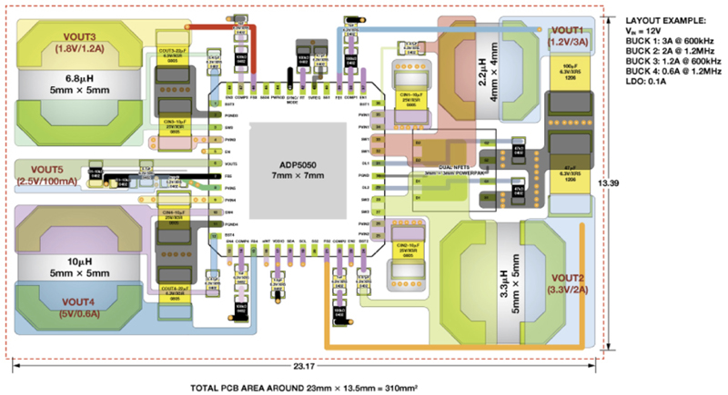
Figure 9. Power supply circuit using ADP5050/ADP5052.
Advanced highly-integrated PMUs are enabling complex power management solutions with high power efficiency, high reliability, and ultrasmall size; and new design tools combined with flexible integrated circuits reduce the time to market for these complex power supplies. Devices such as the ADP505x family, the latest addition to ADI’s portfolio of highly integrated multi-output regulators, allow a single IC to be used quickly and easily in many different applications, reducing power supply design time.