.png)
Power Integrations’ new InnoSwitch5-Pro family can provide over 95% efficiency due to a newly developed ZVS technique that requires no extra components.
USB-C has become the de facto standard for charging around the globe. Helped by regulation, especially in the EU, the protocol has grown until around 5 billion USB PD controllers will be shipped this year, and that figure is expected to almost double by 2028. The market for USB-C charging has expanded from its original target of cellphones and tablets to notebooks and laptops and will continue to grow considerably in other markets, such as home appliances, in the near-term future. Manufacturers want to use USB-C charging in their own designs as it provides them with the ability to focus on one power delivery IC for all of their products. However in some cases the new product may demand more power than is deliverable under the current USB PD standard. In others, the regional standards slightly differ from the main USB-C standard, for example in China, which has adopted the UFCS standard. UFCS is similar to USB-C, but with several differences in how it is implemented.
To give designers the ability to cater for those higher power designs, along with the flexibility to incorporate developing standards, Power Integrations has launched its InnoSwitch5-Pro family of programmable flyback switcher ICs. The company has incorporated an I2C interface into the chips to allow it to be configured by any microcontroller. This allows the microcontroller to handle the different control algorithms, and send the results as a data stream to the InnoSwitch5 chip.
Along with the new interface, the other major change that Power Integrations (PI) has made in the InniSwitch5 family is the incorporation of a new type of zero-voltage switching technique (ZVS). As the name suggests, ZVS is used to reduce voltage to zero before the switch is turned on and the current rises to reduce switching losses. There are several ways to achieve ZVS, but they mainly require additional components to function, making the final design larger, complex and more expensive.
The new ZVS method developed by PI for the Innoswitch 5 family requires no extra components. Andy Smith, Director of Training at Power Integrations explains, “initially, the primary switch is turned off so the voltage across it is high. The secondary synchronous rectification switch is then turned on for a short time, which causes the secondary side of the transformer to energize. The secondary switch is then turned off just before the primary switch is turned on and the charge flips over to the primary side of the transformer and draws current from the parasitic capacitance in the primary switch. Discharging that capacitance brings the voltage across the primary switch down to zero and the switch can be turned on.”
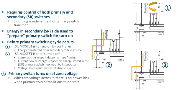
He continued, “The big challenge is to control both the timing of the primary switch and the amount of time that the secondary switch is turned on. There are only a few nanoseconds to make sure the voltage across the primary switch stays at zero at switching. The Innoswitch5 devices have a single master controller on the secondary side that controls both the secondary and the primary switches through the proprietary FluxLink communication link. FluxLink has a finite delay, giving tight control of both switches. This allows the chip to zero-voltage switch without using any additional components.”
The single-chip flyback switcher achieves over 95 percent efficiency through its 750 V or 900 V PowiGaN primary switch, primary-side controller, FluxLink isolated feedback and secondary controller with an I2C interface. The company has demonstrated 140 W / 28 V USB PD adapters in 4.2 cubic inches using only 106 components. The ICs also feature lossless input line voltage sensing on the secondary side for adaptive DCM/CCM and ZVS control to maximize efficiency and simplify design across line and load. A post-production tolerance offset is included to facilitate accurate output constant-current (CC) control of better than two percent to support the UFCS protocol.

.jpg)