Designing for safety, speed, and cost-efficiency in PV inverters
No longer is solar energy an emerging technology, but rather a rapidly maturing one that is undergoing momentous technological changes. The goal of grid parity—where the cost of solar power matches and, indeed, improves that of traditional energy electricity generation types—is getting closer, as the conversion of dc power from the panels to usable ac becomes more efficient and affordable.
But while solar panels have become significantly less expensive in recent years, the next wave of advancement in solar energy will be driven by new technologies for power converter systems. The emergence of advanced and sophisticated multilevel power switching topologies will enable faster power switches based on silicon carbide (SiC) and gallium nitride (GaN) materials and, coupled with higher operating voltages (up to 1600 VDC), deliver a substantial increase in performance over traditional systems. Higher switching frequencies mean that passive elements of the power converter—that is, the inductive coils and capacitors—can be considerably smaller in size, allowing reductions in weight and cost. Both are key advantages in further expanding the markets for solar-based systems.
As a result, these new power-switching topologies are driving changes of the components that control and support them. Smaller, faster systems require improvements throughout the power conversion signal chain—faster processing and better component integration among them. As modern PV inverters get smaller, however, these innovations intensify the challenge of dealing with the significant safety issues inherent in power conversion—that is, as these systems shrink in size, the physical isolation of dangerous voltages becomes more complex.
While solar panels or solar modules are the heart and more obvious part of a solar system, the more complex part of the chain is the PV inverter—the brains controlling the system. The PV inverter needs to be carefully designed to protect the current measurement and computation circuitry from the power-handling circuitry, as well as from transient signals due to switching. But this protection comes at a price: multiple, redundant, isolated components drive up both the cost and the complexity of a system. And, obviously, the incorporation of programmable processors to execute the increasingly sophisticated algorithms required to run these systems are subject to their own safety concerns with regards to code integrity.
In addition, official certification of safety is a requirement that all developers are facing. There are a host of regulations regarding safety disconnects (and reconnects) that must be adhered to. How quickly must a system respond, how are brownouts vs. blackouts handled, rapid disconnects, and arc detection must all be addressed—and in many cases on a country-by-country basis. As certification adds to development time (cost), components and methods with attested conformity are attractive, with the added need to be flexible enough to be able to adapt to multiple and evolving regional safety regulations.
Fortunately, solutions to these problems can be resolved by the utilization of power inverter platforms that integrate advanced mixed-signal control processors, surrounded by complementary isolated current sensing and gate driver technology.
Redundancy—Single-Fault Safety
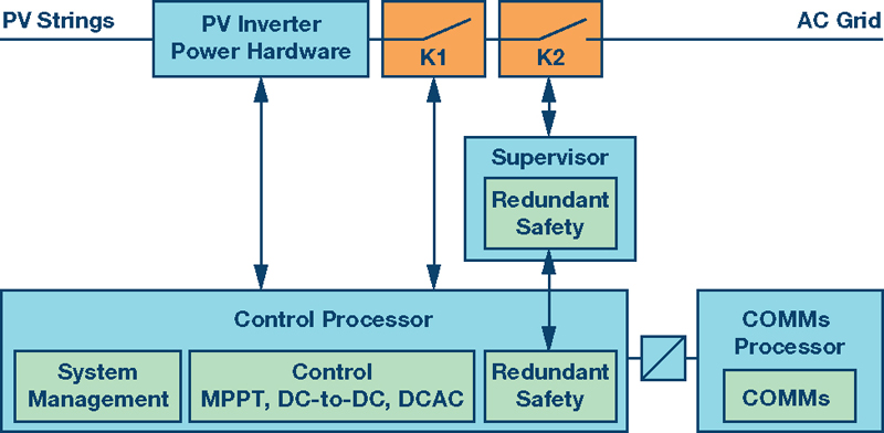
For safety-critical applications such as ac monitors and disconnectors for solar PV inverters, safety standards require a redundant supervisory element besides the monitoring device to ensure single-fault safety. In traditional PV inverters, this is accomplished by adding a supervisor processor to the system, which adopts the role of the redundant monitoring element that then takes control of relay K2 (see Figure 1).

Click image to enlarge
Figure 1. In traditional PV inverter control hardware, a separate supervisor processor takes care of the redundant safety element K2 and the associated monitoring. Both processors run parts of the safety software and communicate via standard I/O facilities.
As can be seen, this adds significantly to the overall costs of the system control hardware, as although the supervisory element actually consists of a processor with rather benign performance requirements, extra supporting infrastructure has to be added as well. On the other hand, this arrangement is favored for its almost visible separation of the redundant elements and hence easy to comprehend safety layout when it comes to conformity audits at safety authorities.
While PV inverter manufacturers are striving for enhanced inverter performance, they are constantly under pressure from worldwide market demands for a lower total operational cost of solar PV systems, and are forced to intensify research on improved inverter topologies and cost reduction on the safety critical parts of PV inverters. Thus, the redundant supervisory element of the safety disconnector becomes a component that is scrutinized with respect to possible cost reduction.
Dual-core design advantages
The desire to simultaneously simplify and enhance the inverter operation led Analog Devices to the development of a series of innovative mixed-signal control processors, the ADSP-CM41x family. Central to the ADSP-CM41x design is its breakthrough dual independent core safety concept, which enables the integration of safety redundancy and functions into a single chip. This first ever architecture saves considerable development time and system cost by eliminating the need for an external supervisory element, which is the current standard.
The new ADSP-CM41x addresses today’s power conversion issues through a set of features that are especially targeted at the requirements of renewable energy conversion systems, including integration of optimized hardware accelerators designed to boost the processing power available for core functions. Additionally, the device’s on-board arc fault detection simplifies design, and enhances safety by using intelligent decision making to improve reliability and accuracy.
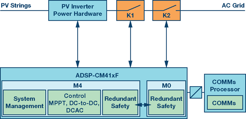
Adding an independent M0 supervisory core to the main M4 control core on a single die, the design of a single-fault-tolerant system with redundant monitoring and control signal paths is greatly simplified while at the same time bringing down overall system costs (see Figure 2).
Click image to enlarge
Figure 2. A dual-core design greatly simplifies the design of redundant safety elements by integrating an independent M0 supervisory core. Processors communicate through a dedicated mailbox system, including the transmission of heartbeat signals.
While an M0 and M4 core share the same silicon—minimizing cost, from a safety perspective—the cores are kept physically, apart through an innovative system fabric design. Inter-processor communication via a dual-ported RAM mailbox allows for independent check and verification of redundantly acquired process parameters.
Code Safety
In addition to physical power safety, great care must be taken to ensure that the algorithms running these systems are being properly interpreted; corrupted processes could lead to safety compromised operational states. Furthermore, it is advantageous to isolate processor-to-processor communications with a mailbox communication system that separates the functions of the processor cores. Rather than a direct transmit-receive handshake method of communications, a mailbox system allows isolated read/write of data by either core at any time.
For code safety, the M4 core has its own 1 MB Flash and up to 160 kB SRAM, while the M0 has its own 32 kB SRAM. The M4 and M0 processor L1 SRAMs, flash memory, and the mailbox memory are all protected with zero wait state SECDED ECC, natively protecting 32-bit memory elements. Writes of 8-bit and 16-bit data, where applicable, will cause automatic background read-modify-write ECC updates, typically with no observable processor stalls. Refresh assist hardware enables periodic scrubbing of single bit errors. Multibit error detections optionally can signal interrupts and/or faults.
Additionally, for error detection, a cyclic redundancy check (CRC) hardware block is used to compute the CRC of the block of data. This is based on a CRC32 engine that computes the CRC value of 32-bit data words presented to it. In particular, the CRC unit can be used to validate the contents of flash memory and of constant blocks of data (text or code) in SRAM.
AC grid monitoring
As an example of how a dual-core design can be utilized, let’s examine how ac grid monitoring works in a PV inverter. AC grid monitoring basically consists of two functions—frequency monitoring and voltage monitoring:
For frequency monitoring, it requires tightly tolerated time-based measurements that can be extremely difficult to achieve when using RC oscillators as a backup timebase. Therefore, the processor uses a single oscillator or crystal (XTAL) as the main system clock (SYSCLK) input and an additional XTAL on the M0 as a monitor against drifts of the main clock source via the mailbox. Clock faults in the SYSCLK line other than drifts are directly handled by the internal oscillator comparator unit (OCU).
The device uses an external low frequency oscillator (LFO) to detect various conditions such as clock dead and clock frequency limit violations and can generate several events to inform the processor about the violations. A clock not good signal (CLKNG) can be configured to put the chip in to a reset state when detecting a fault event, and it can also initiate the GPIO pin safe state mechanism.
AC voltage monitoring has to ensure that phase voltages are within required tolerance bands, and is also used for functional self-testing of the two disconnector relays. To enable single-fault proof voltage monitoring, the processors’ analog front end (AFE) consists of two separate ADC blocks, each comprising its own ADC controller, voltage reference, and multiple supply paths. Of those, one ADC block is controlled by the M4, while the other one is controlled by the M0, allowing for fully redundant voltage measurements and sanity-checks across the mailbox system. On top of that, an on-board DAC can be used to individually exercise internally all parts of the AFE signal chains prior to bringing the PV inverter online.
Putting it all together
In addition to the mixed-signal processor, there are a number of other critical components that need to work together in a PV system to communicate, control, and pass data and current safely.
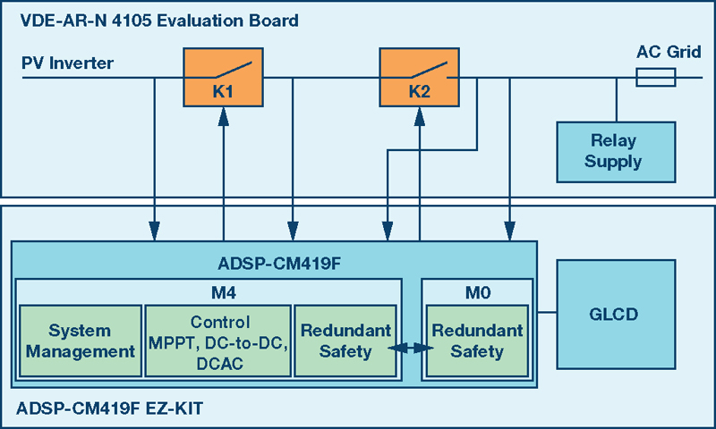
The design features a redundant signal-path concept including redundant references, ADCs, and XTALs, as well as internal oscillator and voltage monitoring units and an inter-processor mailbox system that allow for the complete elimination of additional external supervisory element from the monitoring system (see Figure 3). A graphics LCD delivers all relevant status information at a glance, while a simple push of a button does a full calibration cycle of the entire system. The unit comes with an extensively documented software package and holds an Attestation of Conformity to VDE-AR-N4105 issued by Germany’s TÜV-SÜD in March, 2016.
Click image to enlarge
Figure 3. Block Diagram of the VDE-AR-N-4105 Technology Demonstrator, consisting of the VDE-AR-N-4105 evaluation board and the ADSP-CM419F EZ-KIT.
The future looks bright for solar, but incremental advances are not enough. It is the smart integration of a variety of technologies at the whole platform level that will ensure the efficiency and safety of power converter designs. Each individual component must be specifically designed with the energy market requirements of safety, efficiency, and cost. Providing complete, robust platforms—not just parts—will allow manufacturers of tomorrow’s power conversion products to create clean, safe, and affordable systems.
Safety Attestation
Because cost reduction efforts may easily impair the required safety level of the system, Analog Devices addressed the possible safety issues in a combined effort with German Employers’ Liability Insurance Association BGETEM in Cologne and with TÜV-SÜED in Straubing about how exactly to integrate the supervisory element as a second processor onto the same silicon die of the main processor. An additional consideration was the minimum requirements that such a dual-core processor must fulfill in order to comply with regulatory standards for a safety ac disconnect on PV inverters.
As a result, Analog Devices’ new ADSP-CM41x processor family now holds a Certificate of Compliance to VDE-AR-N4105 (Doc D8 16 03 95142 002), issued by Germany’s TÜV-SÜD in March, 2016. It comes with a set of features that are especially targeted at the power conversion requirements of renewable energy conversion systems, including all necessary safety elements to make up for a fully safety compliant ac disconnector.
Also in support of safety, the Analog Devices power conversion platform incorporates gate drivers and current sensors based on its iCoupler digital isolator technology. ADI’s digital isolators use low stress, thick-film polyimide insulation to achieve thousands of volts of isolation that can be integrated with standard silicon ICs and can be fabricated in single-channel, multichannel, and bidirectional configurations.
Click image to enlarge
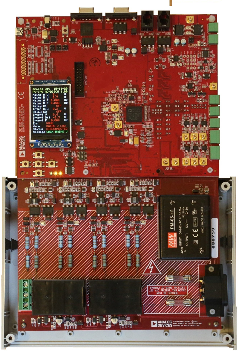
Figure 4. The VDE-AR-N-4105 Technology Demonstrator features two series connected mains relays that form the ac mains power path, plus four independent high precision isolated voltage measurement channels that redundantly monitor ac mains voltage, plus PV inverter output and inter-relay voltages in a single-phase system.


