PassThru Boost Controller for High Efficiency, Fast Transient Response Automotive and Industrial Supplies
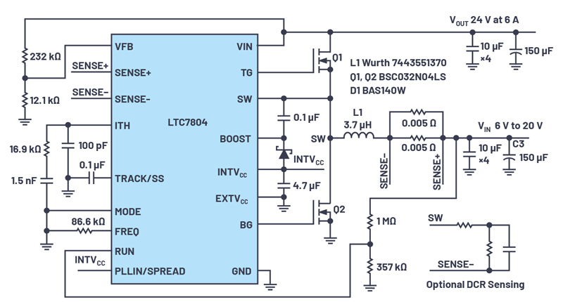
Figure 1. Electrical schematic of the boost converter based on LTC7804 with VIN 6 V to 20 V and VOUT 24 V at 6 A
Boost power supply topology is increasingly popular in automotive and industrial electronics. A significant number of systems require a stable input rail where the upstream supply rail voltage can change significantly. Boost converters can be used to significantly increase application versatility. They enable new electronic equipment to seamlessly connect to any supply rail without requiring front-end redesign or multiple versions to cover various supply scenarios. Boost regulators can also support electronic devices that demand a high degree of rejection against input voltage drops. This is mostly related to automotive electronics where the supply rail can drop significantly—for example, during the cold cranking.
The LTC7804 simplifies the design of boost converters without sacrificing advanced characteristics. The main features of LTC7804 are low quiescent current, single output synchronous rectification, a wide input voltage range up to 40 V where the output can go up to 36 V, spread spectrum frequency modulation (SSFM), and an internal charge pump for high efficiency, low EMI PassThru™ operation.
Boost Converter for 12 V Input to 24 V Output
One of the advantages of a boost converter is that it can provide system immunity to front-end voltage drops, such as from a cranking automobile battery rail, in addition to providing a stable intermediate output rail. Figure 1 shows the schematic of a boost converter consisting of a low pin count controller LTC7804, bottom FET Q1, top FET Q2, chock L1, and input/output filters. The schematic features a low component count solution, but can boost a 12 V rail to 24 V and deliver 6 A of the output current. The output current should be derated at low input voltages to keep input current below 17.5 A.
In this particular solution, the MODE pin is connected to GND, invoking Burst Mode®operation, which maintains high efficiency at light loads. The PLLIN/SPREAD pin is connected to INTVCC, setting the switching frequency to SSFM operation, which eases the qualification against published EMI standards. This design was tested using dedicated current sense resistors, but it can operate entirely without current sense resistors, using optional DCR sensing instead. The efficiency of this solution is shown in Figure 2.
Click image to enlarge
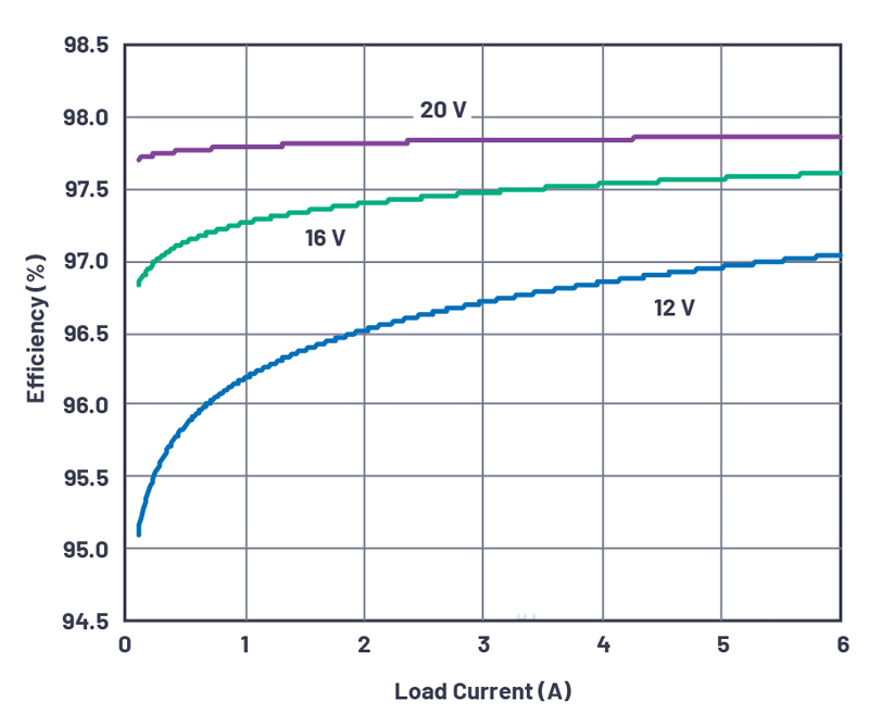
Figure 2. Efficiency curves of the boost converter on Figure 1
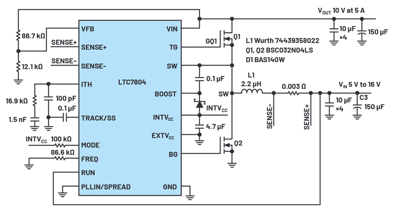
Rejection of the Input Voltage Drops and PassThru Mode Operation
One interesting application of the LTC7804 is supplying automotive audio amplifiers and preamplifiers. The goal of this application is twofold. First, the LTC7804 rejects sudden drops in the input voltage—for example, during cold cranking. Second, it essentially shorts the input to the output when input voltage rises above the output level to maximize efficiency, such as during load dumps. The voltage output of a preamplifier power supply is set to a value a little less than the automotive rail voltage (around 10 V) from the typical 12 V automotive voltage rail. If input voltage is equal to or above the set value, then the input should pass directly to the output. If the input voltage drops below the desired intermediate voltage, the boost converter keeps its output at the set value. The term PassThru is used to describe this direct input-to-output mode of operation.
Figure 3 shows a complete schematic for the boost solution. It’s similar to the solution shown in Figure 1, but the connections of the control signals are slightly different. The MODE pin is connected to INTVCC through a 100 kΩ resistor to select pulse skip operation. Burst Mode operation is not supported in this application, because to enable PassThru operation, the top MOSFET gate charge pump must be enabled—it is disabled in Burst Mode operation. The PLLIN/SPREAD pin is tied to GND to disable the SSFM feature, as it is important for the power supplies for some audio systems to operate at a fixed frequency. If knowing the frequency is a real concern, then synchronization to an external clock through the PLLIN/SPREAD pin is advised; that, or connect the MODE pin directly to INTVCC to select forced continuous conduction mode at the operating frequency set at the FREQ pin.
Click image to enlarge
Figure 3. The boost converter is able to operate in PassThru mode, with VIN 5 V to 16 V and VOUT 10 V at 5 A
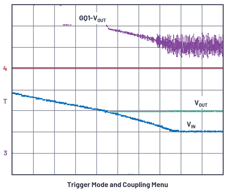
Figure 4 shows how the solution functions through operational waveforms. In the test, the input voltage starts at 14 V, above the preset converter output of 10 V. The gate of the top MOSFET Q1 is high and Q1 is ON—it is completely enhanced. The LTC7804 internal charge pump can keep a converter in this state indefinitely. This is PassThru mode, where there’s no switching action, with the input voltage passed directly to the output at 14 V. PassThru mode is enabled as long as the input is above or equal to the desired output as shown in the waveforms. The output voltage holds at 10 V even as the input drops to 5 V. The switching action begins once the input drops below a preset value to keep the output exactly at this level. The GQ1-VOUT waveform is the differential voltage on the Q1 gate (GQ1 node) relative to Q1 source (VOUT).
Click image to enlarge
Figure 4. PassThru operation at VIN > VOUT. VIN , where VOUT 5 V/div, the time scale is 1 ms/div, and GQ1-VOUT is the oscilloscope’s mathematical function with 2.5 V/div.
The switching frequency of both converters is around 500 kHz to balance efficiency and size, but can be increased to 3 MHz if the inductor (L1) size must be minimized. Both solutions presented in this design note were verified and tested on DC2846A.
Conclusion
The LTC7804 controller significantly simplifies the design of highly efficient boost converters. Available output power is easily scaled by employing the same schematic and changing external components. The high switching frequency enables significant reduction in the size of the inductor. The internal charge pump and synchronous rectification guarantee maximum efficiency when the input voltage drops far below or rises far above the output level, making the LTC7804 an ideal controller for automotive electronics. Low quiescent current also preserves battery life in automotive and always-on systems.