SiC FETs enable very low static and dynamic losses in power conversion due to their low on-resistance and ultra-fast switching. However, these characteristics also make PCB design critical to avoid component stress and EMI noises.
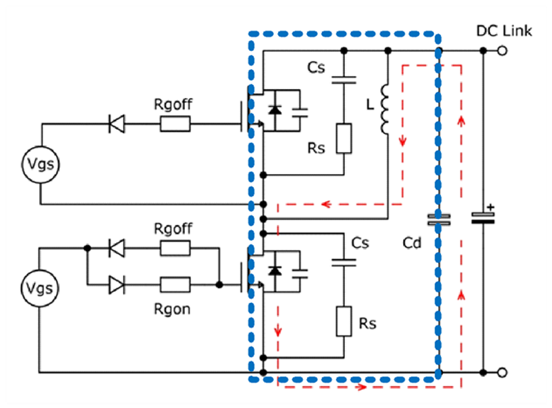
Figure 1: The loop from switch to DC link capacitor can be long and have significant inductance
Optimising PCB layout in a power converter design is a complex task at the best of times, but there can be extra challenges when you have to allow for the ultra-fast voltage and current edge rates seen with wide band-gap devices such as a SiC FET, a normally-off, cascode combination of a SiC JFET and Si-MOSFET. The problems arise from the interaction of fast dV/dt and di/dt with parasitic circuit capacitances and inductances. Values that would produce negligible effects with slower-switching IGBTs or even Si-MOSFETs can result in induced currents and voltages that can at best cause chaotic operation and at worst device failure.
WBG devices have rapid edge rates
Putting a scale to the challenge, a SiC FET can easily switch current with an edge rate of over 5000A/µs and if the loop inductance, from the switch to local decoupling capacitors is significant, a voltage transient is produced according to E=-L.di/dt, for example, 250V from 50nH for 5000A/µs (Figure 1).
This voltage adds to the switch operating value, at best reducing margin to breakdown. This might seem like a high inductance value, but power components usually can’t be packed close together and this inductance would appear from only about 60mm of total PCB ‘go and return’ track length (l), 2.5mm wide (W) and 0.07mm thick (T), calculated from the equation derived by Terman:
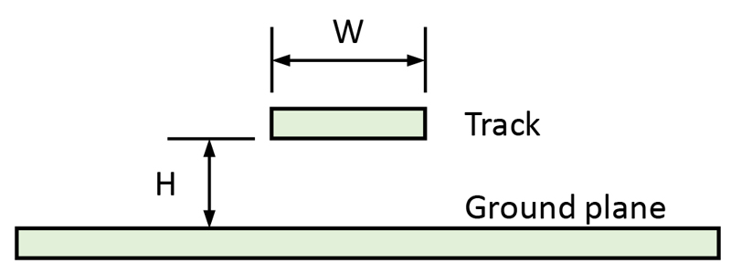
The relationship shows that it is important to maximize track width and thickness and minimize the distance to decoupling capacitors for minimum inductance. If the DC link capacitor in Figure 1 is not close and is a large component which might have high inherent self-inductance, a smaller high frequency capacitor should be fitted, Cd, close to the switch. Inductance is also minimized if the enclosed area of the current loop is small. This can be effectively achieved with a ground plane under high frequency power tracking, forming a return current path. If this is implemented as a 2.5mm wide track (W), with a ground plane on the bottom side of a 1.6mm thick (H) PCB (Figure 2), the loop inductance for 60mm total length (l) would reduce to about 20nH, according to the equation from Clayton:
The equation applies for W/H>1. With ground planes above and below the track, the inductance reduces further still.
Click image to enlarge
Figure 2: A return ground plane below a track reduces its inductance
If possible, PCB via connections should be avoided for the power path due to their voltage drop, but they also add some inductance. The value depends on the physical arrangement and whether filled or not, but an approximate figure is 0.5nH for 0.5mm diameter and 1.6mm length. In practice, vias in a power path are typically paralleled, reducing inductance to an overall lower value.
Gate return and source connections should be separated
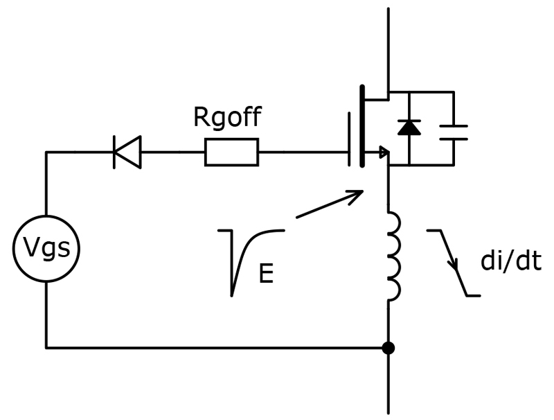
High current edge rates in the source of a SiC FET should not be allowed to couple into the gate drive loop (Figure 3). Common inductance causes a voltage spike with source di/dt, which opposes the gate drive signal and potentially cause ‘phantom’ turn-on, shoot-through in bridge ‘legs’ and failure. With three-lead TO-247 SiC FETs, the gate drive return connection should be as close as possible to the source pin to minimize common inductance, but a limitation is the inherent package inductance of the source lead of about 10nH. As a solution, four-lead ‘Kelvin connection’ devices from the UnitedSiC (now Qorvo) range of SiC FETs can be used to reduce the value to the die figure of around 1nH. With this arrangement, SiC FETS can then safely be switched faster with a consequent reduction in dynamic losses.
Click image to enlarge
Figure 3: Common inductance in the source and gate drive loop of a SiC FET causes gate voltage transients with current transitions
Capacitance can be a problem as well
Wider tracks reduce inductance, but increase capacitance to adjacent connections and ground. This can pose a problem with high voltage edge rates. dV/dt values of 100kV/µs are easily achieved with SiC FETs and are seen as a way to reduce switching losses, but induced displacement currents can be high. For example, with this edge rate at a switching node and 10pF stray capacitance, a displacement current of 1A could flow, taking an often-indeterminate return path. The switching node is typically the source connection of a high-side SiC FET and a relevant capacitance is across its gate driver isolation barrier, both signal and power. To minimize problems, the optocoupler or magnetic isolator used, along with any DC/DC converter supplying gate drive power, should be specified to have a low capacitance, in the order of a few pF in total, along with a high common-mode rejection ratio. Other tracks around the switching node should also be kept at a distance to minimize coupling capacitance and pickup, and any sensitive feedback or control connections should certainly be kept as far away as possible.
Capacitance from a SiC FET switching node to a PCB ground plane or grounded heatsink will induce high-frequency common mode currents which can affect ability to pass statutory levels for conducted emissions on the input supply, particularly relevant with AC input converters. One solution is to interpose an electrostatic screen, connected to the switching return or DC supply voltage and this can be formed from a discrete, insulated copper sheet or it could be a PCB plane. However, this will add some thermal resistance to the path to the heatsink or PCB, increasing junction temperature for the same power.
Thermal considerations
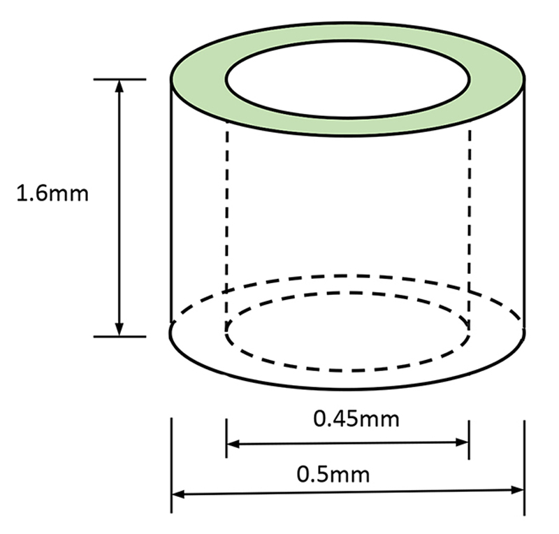
Power switches increasingly rely on heat dissipation into PCB tracking, as designers realize that efficiency gains with devices such as SiC FETs avoid the necessity for costly and large external heatsinks. The heatsinking effect of PCB planes and tracks is difficult to evaluate due to interactions with other components, but it can be estimated using multiphysics simulation packages. The result is influenced by the number of PCB layers, PCB material, copper weight, airflow rate and direction, surface emissivity and cross heating from other components. Thermal vias can be used to transfer heat between PCB layers, producing lower thermal resistance than relying on flow through an FR4 PCB core, with its thermal conductivity of about 0.25W/m-K. An unfilled via 1.6mm long, 0.5mm diameter with a wall thickness of 0.025mm has a thermal resistance of about 100°C/W (Figure 4).
Click image to enlarge
Figure 4: A typical via has a thermal resistance of about 100°C/W a resistance of about 0.7 milliohms and an inductance of about 0.5nH
If a 25mm square PCB area is considered, thickness 1.6mm, with copper on both sides, it will have a thermal resistance of about 8°C/W from top to bottom, which could be halved with just 12 thermal vias. Insulated metal substrates (IMS) have around 45% lower thermal resistance than FR4, but are more costly with fewer layers economically available. Dielectric thickness of IMS is typically 0.15mm per layer to minimize thermal resistance, but this does increase capacitance from the attached device to the metal substrate, with the danger of high common mode currents as already described. IMS arrangements suit high-density applications where temperature rises must be minimized and forced air or liquid cooling is available, whereas relying of FR4 with thermal vias to a heat-dissipating plane or sink more suits convection-cooled systems.
Latest generations of switching devices are increasingly available with top-side cooling as an option which places less reliance on the thermal performance of the substrate.
While the switching device such as a SiC FET will be the main heat-producing component, associated snubber networks will also dissipate some power. The snubber should be as close as possible to the switch for best effect to minimize voltage overshoots and can typically consist of a surface-mount series resistor and capacitor. Tracking around the components should be sufficient weight to dissipate the snubber power and the effect of conducted heat from the main switch should also be considered. A thermal break in the tracking to the snubber could be useful.
PCB tracking resistance should be kept low
Devices such as SiC FETs are achieving milliohm-level on-resistances at high voltage ratings and to keep the advantage, PCB tracking to the device should be as low resistance as possible. Losses and heating in PCB track resistances can be evaluated from copper resistivity, thickness and the total number of ‘squares’ in any dimension along the whole track. For example, 35µm/1oz copper has 0.5 milliohm resistance per ‘square’ so a 2.5mm wide track 2.5mm long has the same resistance as a 10 mil wide track 10 mil long. If tracking were 2.5mm width therefore, just 50mm length would measure 10 milliohms, comparable with the SiC-FET on-resistance. Copper resistance increases linearly with temperature, about 30% between 25°C and 100°C, which should be accounted for in loss calculations.
Power designers will be familiar with the ‘skin’ effect where high frequency currents concentrate on the surface of conductors. The skin depth is around 66/f1/2 mm,but with typical PCB tracking to power devices, the effect is small. Even at say, 1MHz switching, with most power in the fundamental frequency, the current flows to a depth of about 0.07mm, or the full thickness of 2-ounce copper.
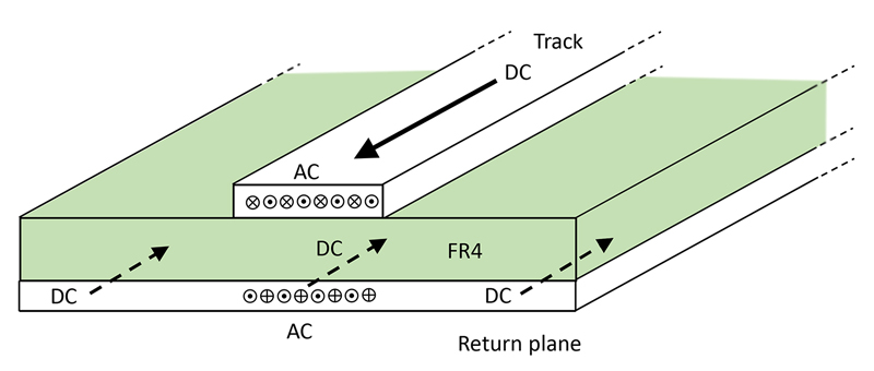
A related effect which is non-trivial, is the way current returns through a ground plane. High-frequency current does not spread out but follows a path in the ground plane directly under the power connection, (Figure 5). This means that the effective resistance around the complete current loop may not be as low as expected, although the scale of the effect depends on the waveform and any DC component, which will spread out further.
Click image to enlarge
Figure 5: AC return current in a plane is concentrated below a track. Any DC component spreads further
Conclusion
SiC FETs are approaching the ideal, with fast switching and low on-resistance. However, real-world connections to the devices with parasitic inductance, capacitance and resistance also need to be considered to realize potential performance gains.


.jpeg)