Power Supply Considerations
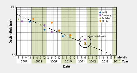
The handset world is seeing a burgeoning need for memory storage. This article discusses memory trends and different methods of powering SD Flash memory. The need for memory is being driven by rapid advancements in the ability to capture, display, and share both video and image content. Capture is making huge strides due to the emergence of miniaturized camera optics, highly integrated image processing, and flashes both in the form of increasingly bright LED solutions and shrinking xenon solutions. Thin and efficient touch screen LCD, AMOLED, and Super AMOLED solutions mated with intuitive user interfaces have made displaying photos and videos a simple and vibrant experience. Finally, sharing has been accelerated due to ubiquitous connectivity, social networks, and numerous sources of downloadable content. These technologies are driving and enabling cell phone manufacturers to design phones with cameras capable of 8 or even 12MP image resolutions. Or in the case of video we are increasingly seeing cell phones with the capability to shoot 720p@30fps. These are all memory- intensive applications and typically this content is stored in the form of solid state memory. While digital still cameras have historically demanded large memory capacities, this requirement for cell phones has only become prominent in the last few years. Fortunately though for the consumer, solid state memory density and production capacity have been increasing over time leading to significant reductions in both price ($/MB) and area (mm2/MB). Figure 1 illustrates that in 2011 process geometries will likely breach 25nm for NAND-based flash memory.
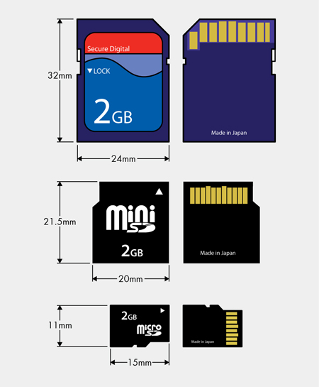
The most common solid state memory format for consumer storage applications is SD Flash. Modern day SD Flash memory is based on NAND technology and comes in the three form factors SD card, mini SD card, and micro SD card shown in Figure 2. Though the three form factors differ in size they do not differ in electrical interface.
Independent of form factor, SD memory is also categorized based on capacity range. Standard SD cards provide a maximum of 2GB capacity, high-capacity (SDHC) cards have a capacity range of 2 - 32GB, and eXtended Capacity (SDXC) fall in the range of 32GB to 2TB. There are also two clock rate categories. In default mode, the memory can operate with a clock rate range of 0 - 25MHz providing up to 12.5MB/sec interface speed (using 4 parallel data lines). In high-speed mode, the memory can operate with a clock rate range of 0 - 50MHz providing up to 25MB/sec interface speed (using 4 parallel data lines). It is up to the system designer to optimize this parameter based on the desired read and write speeds. This matter becomes important when we get to the discussion of power supply considerations.
SD Specification Version 2.00 calls for an operating voltage supply range of 2.7 - 3.6V. 2.7V is defined as the minimum voltage required for guaranteed performance. Above that and up to 3.6V is acceptable but is also unnecessarily wasting power. Beyond 3.6V, performance is not guaranteed and in addition the memory is at risk of being damaged. Another consideration for the power supply design is the current consumption of the memory. Current consumption varies depending on which of the four main states the memory is in: shutdown, standby, read and write. For a given memory card, read/write current consumptions can also vary depending on the rate at which data is being clocked into or out of the memory. Regular cards support clock frequencies of up to 25MHz and high speed cards can support up to 50MHz. As capacities become larger, it becomes apparent that fast clock rates are desired in order to ensure reasonable usage models for the consumer. Small capacity SD cards operating at low speeds often consume less than 100mA. Given that Li-Ion batteries nominally operate at 3.7V and that memory supply rails are quite high, linear regulators have become the incumbent power supply of choice for SD memory. The selected linear regulator though has to be capable of operating with low drop out because the Li-Ions have an effective voltage range of 3.2 - 4.2V. With the emergence of 8, 16, and 32GB high speed SD cards, it is not uncommon to see current consumptions in the range of 300 - 400mA. These current levels are substantially higher than the 100mA of the lower capacity cards. At these new increased current levels, LDO power supply solutions begin dissipating substantial amounts of power. Figure 3 shows an LDO powering an SD card at a typical voltage of 2.9V. 2.9V is chosen with the assumption that the LDO can guarantee its output will never drop below 2.7V under any line, load, or temperature conditions.
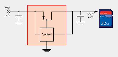
Table 1 calculates conversion efficiency for the LDO scenario in Figure 3 at current levels of 300 and 400mA. The conversion efficiency of the LDO is 78% resulting in power dissipation of 240 and 320mW respectively.
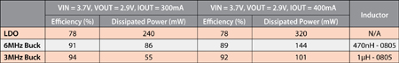
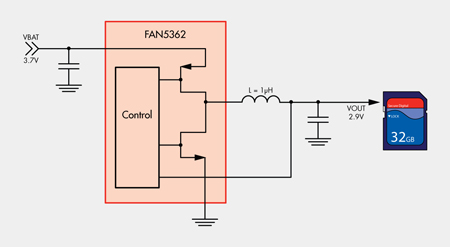
Many system designers will understandably find 320 and even 240mW power loss to be unacceptable. Fortunately it is possible to use a switching converter as shown in Figure 4 to achieve higher power conversion efficiency.
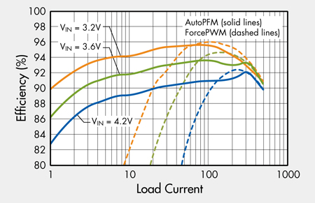
As calculated in Table 1, the FAN5362 can reduce dissipated power down to 55mW for the 300mA system and 101mW for the 400mA system. These efficiencies are based on measured efficiency curves taken on the FAN5362. Figure 5 below shows these curves for both AutoPFM (solid line) and ForcePWM (dashed line). While optimizing the FAN5362's efficiency, 3MHz was selected as the nominal switching frequency because it provided the best tradeoff between size and efficiency. As can be seen in Table 1, using a 6MHz switcher in this power conscious application dissipates considerably more power than a 3MHz switcher.
While the selection of a buck to replace an LDO may seem trivial, it is important to consider that the buck must be capable of operating at very high duty cycles. If the buck's output is set to 2.9V and the battery has come down to 3.3V, the buck is already operating at 88% duty cycle. At some conditions of load and input voltages the buck will even be forced to stop switching and operate at 100% duty cycle. The situation gets even worse during low VBAT situations if the phone starts transmitting GSM pulses. GSM pulses can be as high as 2A and during these pulses the output impedance of the Li-Ion battery will cause the battery to drop by as much as 400mV. For LDOs this sudden VBAT drop is palatable because LDOs are always operating in the linear region. It is a different situation though for buck converters because they must gracefully transition from switching to 100% on and then back to switching again once the battery returns to 3.3V. During the phase in which the high side device is fully on, the output voltage of the buck is simply VBAT - RDS(ON) *I - DCR*I where RDS(ON) is the on resistance of the high side FET, DCR is the series resistance of the inductor, and I is the memory load current. The FAN5362 was designed to handle the scenario described above with minimal over and undershoot. In addition, the control mechanism and RDS(ON) of the FETs were carefully designed such that the output voltage can be guaranteed to never drop below 2.7V, even including both line and load transients. This is critical for memory because SD Specification Version 2.00 calls for an operating voltage supply range of 2.7 - 3.6V.
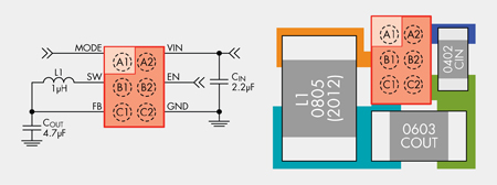
Figure 6 shows a typical schematic and PCB of the complete FAN5362 power solution. While process geometry advancements address the need for ultra compact and affordable SD memory, the resulting high capacity devices also present a power consumption problem. This problem can be overcome by replacing the incumbent LDOs with a buck converter such as the FAN5362, which was designed specifically for this application. www.fairchildsemi.com