Grid-tied PV inverter using PV-IPM
This article describes a dual input two stage grid-tied PV inverter by using Mitsubishi Photovoltaic Intelligent Power Modules (PV-IPM) of type number PM50B6LA060. Dual circuit branches have independent boost converters and tracking control of maximum power, which can be connected with various PV arrays and make the PV system easy to use. Small and decentralized power supplies such as used for photovoltaic generation, wind power generation, and fuel cells are in greater demand due to the rise in environmental concern. In addition, an increase in the use of domestic photovoltaic generation systems and fuel cell systems is expected in future. Because the voltage generated in these systems is DC, it is necessary to convert the DC voltage into an AC voltage for use in the home. The device used for the DC-AC conversion is a power conditioner, and a semiconductor power device is used within such a system. High Efficiency is needed in the power conditioner, and so a semiconductor power device with low loss is requested. Mitsubishi Electric Co., Ltd has developed an IPM for the photovoltaic generation to have satisfied such a demand. The internal circuit of a photovoltaic intelligent power module (PV-IPM) is shown in Fig.1. It integrates single phase output inverter circuit, two chopper circuits (one chopper circuit for some types and without chopper circuit for other types) and control IC into a small package. The PV-IPM adopts an innovative CSTBTTM chip technology to achieve low power loss. There is a thermal sensor mounted on the surface of each IGBT chip so that junction temperature (Tj) can be monitored accurately.
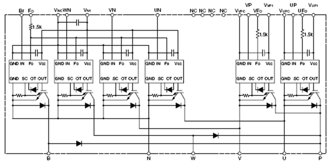
The PV-IPM has short circuit protection, control supply under voltage protection and over temperature protection. When the PV-IPM module detects overheating (OT) or load (the arm) short circuit (SC) or control supply under voltage (UV), an immediate controlled shutdown is initiated and a fault output is generated and indicated through Fo terminal. In addition, the internal control IC can adjust gate charge according to measured collect current in order to decrease radiation noise. A prototype Grid-tied PV inverter applying such a PV-IPM has been designed. The type name of the PV-IPM is PM50B6LA060. The structure of the system and the control approach of the grid-tied PV inverter are presented in the following paragraphs. Furthermore, the grid current and voltage based on the prototype have been measured. Structure of the Grid-tied PV Inverter The main circuit topology of PV inverter system is shown in Fig.2. PVa and PVb are independent PV battery arrays; L1 and L2 are boost inductors; C1 and C2 are filter capacitors; C3 is the DC bus capacitor; L3 is a filter inductor of inverter. The inverter is connected to the grid by a power frequency insulation transformer T1.
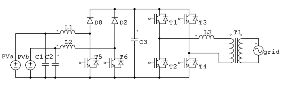
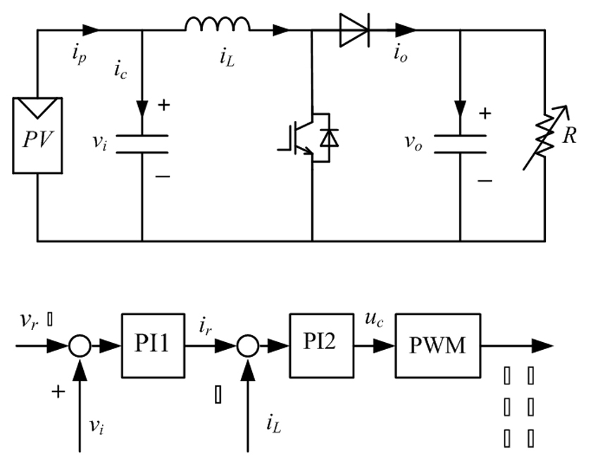
This circuit has several features. Firstly, the boost system consists of two independent boost converters which can work under various input voltage or input power to meet different requirements of customers. Both input battery boards of dual circuit branches can be mounted in different directions according to actual environmental requirements. If there is only one PV battery board, it can be connected with each of dual circuits. Secondly, the output of dual boost converters is gathered by the DC bus capacitor and connected to the grid through inverter. Finally, each boost has its own maximum power tracking control to make the system operate at the maximum power situation and improve the system efficiency. Control Approach The control approach of front stage boost converter is shown in Fig.3. In Fig.3, vi and vo are input and output voltage respectively; iL is current flowing through the inductor. The input reference of voltage loop control, vr is the voltage operating at maximum power and it could make the input voltage of boost inverter quickly reach the value at the maximum power situation. The converter can boost low DC voltage of photovoltaic array up to high DC voltage and transfer the electrical power to the DC bus line. The backstage inverter can keep the DC bus voltage stable by adjusting power injected into the grid. In other words, the load of the boost converter is the DC voltage supply. The Boost converter can realize tracking control of maximum power by changing the input voltage to adjust the photovoltaic array operating points.
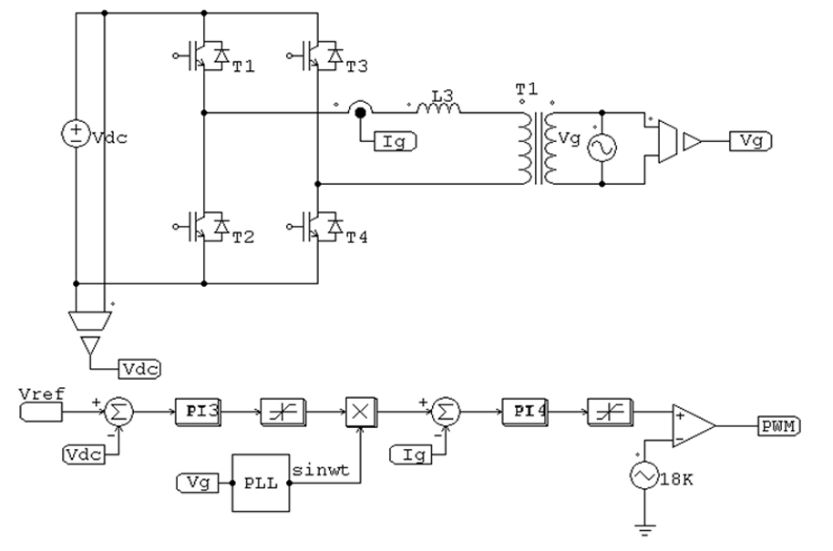
The backstage inverter works in current control mode. The grid-tied current or grid-tied power is dependent on the closed loop of the DC bus voltage. The control loop of the backstage inverter is shown in Fig.4. Vdc is the bus voltage and a feedback signal of voltage control loop of the back stage inverter. Vg is the voltage of the grid. The phase information of the grid voltage and reference phase of the grid current could be obtained through phase locked loop (PLL). Ig is output current of inverter and as feedback signal of the current control loop. The output of voltage control loop is the reference of grid current magnitude. However, the magnitude and the phase of the current injected into the grid are controlled by the current control loop. When the grid current magnitude is higher than the limit value, the over current protection function will be activated. This dual closed-loop control system can result that harmonic content of the inverter is lower than 3% and power factor of the inverter combined to the grid is higher than 0.99.
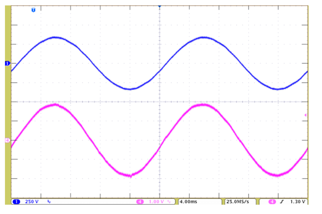
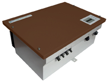
The power management system of the two stage grid-tied inverter is very important. The Boost converter can transfer power generated by the PV array into the DC bus with the maximum efficiency. If the total input power from two branches is higher than the maximum output power of inverter, the inverter can be locked by over current protection to limit the grid-tied power. If the input power of DC bus is higher than output power, the DC bus voltage may rise to trigger over voltage protection. The relationship between front stage power and back stage power can be recognized by monitoring the change of the bus voltage and limitation state of the output current. The trace control direction of maximum power of the front stage boost converter is reversed to decrease the input power and keep the DC bus voltage stable when output current is on limiting situation. Prototype of the Grid-tied PV Inverter and Test Results Waveforms shown in Fig.5 are test results of a 3kW grid-tied PV inverter under 230V/50Hz power grid and 390V DC bus voltage. The THD of grid current in the test is 1.24%. Also, outline of the 3kW inverter and conversion efficiency versus PV voltage and power is shown in the Fig.6 and Fig.7 respectively.

Conclusions PM50B6LA060 is convenient to be used in middle or low power single phase PV inverters with high efficiency. Dual DC input can be connected to PV arrays with different voltage and power specifications. Dual circuit branches which have independent DC-DC converters and tracking control of maximum power do not require identical input and can be easily located in a PV system. The front stage boost converters are controlled independently by the same closed-loop control method and the inputs of dual circuit branches are boosted to the same bus voltage. The output power of dual circuit branches is gathered by the bus capacitor and connected to the grid by back stage inverter. The back stage inverter module is controlled by voltage outer control loop and current inner control loop. The well designed loop control system can achieve low harmonic content and high power factor. Two-stage grid-tied inverter can bring reliability to the energy management system.


