Power ICs Integrate Fast, Autonomous, Precise Protection Circuits for Ultimate System Robustness
Power supply designs continue to push the boundaries for higher power, higher frequency, and higher power density
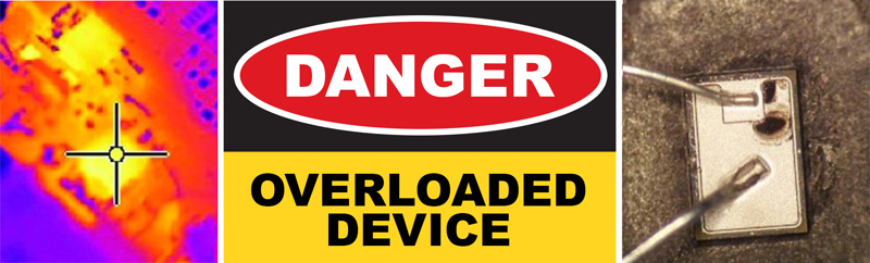
Figure 1: Device overload causes high temperatures and destruction
As maximum load requirements increase and size decreases, the current, power and thermal stress also increases for the power switching device. The need to protect against overload conditions becomes paramount. As switching frequency increases, the need for faster fault detection, reaction, and protection times becomes critical to prevent damage or destruction. The latest GaNSense Power IC protection features are specifically designed for ultra-fast detection and protection against various fault conditions. This article explains each fault condition and shows how GaNSense power ICs detect and protect against these overload events.
Danger! Device Overload!
Every designer’s worst nightmare is a damaged power supply. This can consume endless resources and schedule delays to perform the failure analysis, find a solution, manage resulting product recalls, and minimize customer downtime. If the switching device is damaged, then it was most likely caused by an overload condition. A series of events usually occurs that eventually leads to thermal overload and destruction. Assuming the unit is running under worst-case conditions (low AC line input, 100% load, and the highest ambient temperature), the current ramps up in the device during a normal switching cycle. The I2R conduction losses increase, causing the junction temperature (TJ) to increase. As the current increases further, the device will start to saturate, and the device's current and voltage will instantly increase to a very high level before any over-current protection circuit can react. The resulting power loss and TJ increase so high and so fast that the package and heatsinking cannot dissipate the heat in time for the main circuit fuse to open first. The package then cracks or explodes, causing smoke or fire, and the unit stops working. A truly reliable protection solution against device overload requires multiple protection circuits to detect over-current, saturation, and over-temperature fault conditions and shut down safely before destruction occurs.
Over-Current Protection (OCP)
Over-current protection is a safety feature that is designed to prevent damage to a device or circuit by limiting the flow of current. In the case of GaN devices, over-current protection is particularly important due to the high switching speeds and high-power density of these devices. If an over-current event occurs, it can cause significant damage to the GaN device and may even result in its failure. An external current sense resistor is usually placed in between the source of the power FET and ground, and a comparator and threshold voltage are used to detect when the voltage across the current sense resistor exceeds a maximum limit (Figure 2). Should the current exceed this maximum limit, the comparator output is then used to disable the power FET gate driver to turn it off safely before any damage can occur. This method typically has a long delay time (300 nsec) and is commonly used for Silicon FETs running at low frequencies (<100 kHz) where the OCP circuit has enough time to detect and turn the power FET off before the current can over-shoot and cause damage. This delay time is also needed to blank out any false triggering due to parasitic inductance spikes that can occur due to the external current sensing resistor and PCB traces. At higher switching frequencies, the current ramps much faster each switching cycle, so the speed of detection becomes critical. Due to the minimum blanking delay time needed with external current sensing circuits, this method is inherently limited to lower frequencies. Another solution is needed that can detect and protect much faster and is not susceptible to parasitic noise spikes.

Click image to enlarge
Figure 2: Integrated GaNSense OCP vs external OCP simplified circuits and timing diagrams
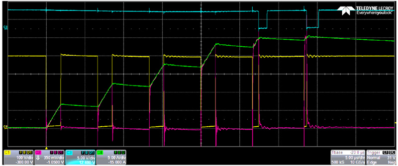
To improve the OCP function, GaNSense power ICs integrate autonomous, cycle-by-cycle detection and protection circuitry together with the GaN power FET and gate driver (Figure 2). This dramatically minimizes the delay time needed to detect the fault and minimizes the delay time to react and shut down the power FET. Also, because the current sensing is also integrated, the parasitic inductances and noise spikes are now eliminated, so the required blanking time is minimized. The result is an OCP circuit that reacts six times faster than the traditional external method. This real-time, instant solution detects and protects within 50 nsec and reduces the peak current over-shoot to a nearly negligible level. Figure 3 shows the NV6169 GaNSense power IC waveforms during an OCP event. The current ramps up each cycle to a higher peak level as the internal GaN power FET is turned on and off with the PWM input. When the CS pin output exceeds the internal 1.9 V threshold, the internal gate driver is turned off instantly, and the on-time period is truncated. The cycle-by-cycle OCP circuit will continue to truncate each on-time period when the over-current event occurs to limit the maximum current level and safely protect the device (and external circuit) from damage. The NV6169 also includes a fault output pin (FLTN) that goes low each cycle when the over-current event occurs. This signal can be fed back to the system controller so it can decide if it should shut the complete unit down on the first pulse or wait until several sequential OCP events have occurred.
Click image to enlarge
Figure 3: NV6169 GaNSense power IC cycle-by-cycle OCP waveforms, IL = green (5 A/div), VDS = yellow (100 V/div), CS = red (0.35 V/div), FLTN = blue (5 V/div), time = 5 µsec/div
Avoid Saturation! Avoid the Runaway!
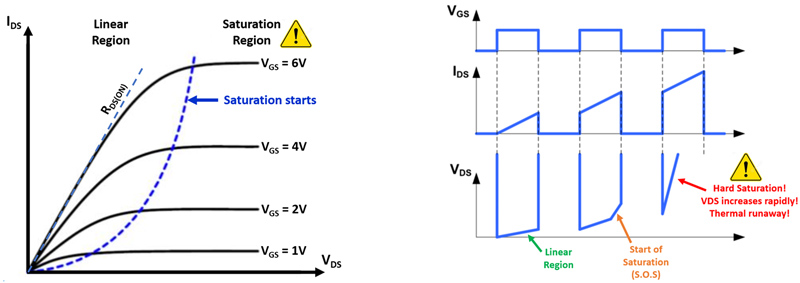
Similar to silicon FETs, GaN power FETs also have linear and saturation regions of operation (Figure 4). When the GaN power FET is in the ON state and the VGS voltage is at a fixed level (i.e. 6 V), a current will flow from the external switched-mode power supply circuit, through the drain, and to the source. The IDS current and VDS voltage levels are low enough such that the GaN power FET operates in the linear region where the VDS voltage changes linearly with the IDS current with a slope equal to RDS(ON). The i2R conduction power losses and resulting thermals are at acceptable levels. Should the IDS current levels start to increase to higher levels due to an overload condition, the device will start to enter the saturation region. The I-V curve starts to flatten, and the VDS voltage starts to increase very rapidly. The resulting conduction losses and device temperature will also increase rapidly. As the device temperature increases, the device will go deeper into saturation, causing higher losses and higher thermals. This "thermal runaway" condition will cause the device to become damaged or self-destruct.
Click image to enlarge
Figure 4: GaN FET linear and saturation operating regions
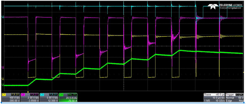
To protect against saturation, GaNSense power ICs include a short-circuit protection circuit (SCP). This circuit differs from OCP in that it detects the VDS voltage instead of the IDS current. The VDS(ON) voltage is measured during each on-time period of the GaN power FET and compared against an internal SCP threshold voltage. During a short-circuit event, the device will saturate, and the VDS(ON) voltage will increase very rapidly to a high level and exceed the SCP threshold voltage. The internal comparator will detect the high VDS(ON) voltage and shut down the GaN power FET instantly, truncating the on-time before thermal runaway or damage can occur. This SCP detection adds another level of robustness and reliability to the GaNSense power IC since it will always detect and protect against saturation, even as the saturation point moves with temperature. Figure 5 shows the NV6169 GaNSense Power IC waveforms during an SCP fault event. As the current increases each switching cycle, the device eventually saturates and the VDS voltage increases rapidly. The integrated cycle-by-cycle SCP protection circuit instantly shuts down the GaN power FET safely to avoid damage. The FLTN output also goes low each cycle during an SCP fault event and can be used by the system controller to decide how the system should react.
Click image to enlarge
Figure 5: NV6169 GaNSense power IC SCP protection waveforms. IL = green (20 A/div), VDS = yellow (100 V/div), VDS clamped = red (2 V/div), FLTN = blue (5 V/div), time = 10 µsec/div
Over-Temperature Protection (OTP)
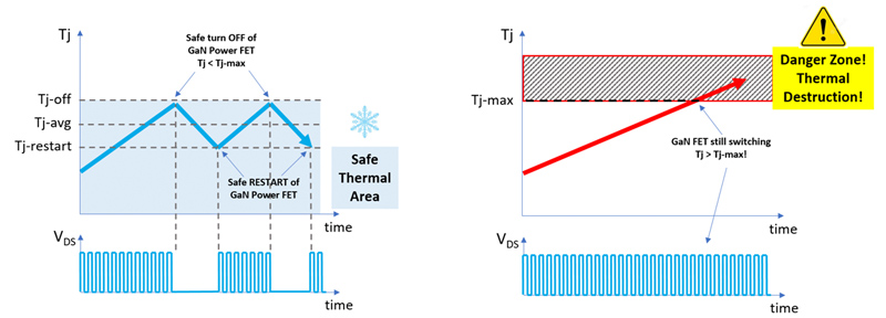
To further increase reliability and robustness, GaNSense power ICs include integrated over-temperature protection (OTP). Traditional OTP circuits are placed externally on the PCB and located far away from the power switch. These are typically used to detect an over-temperature condition in the ambient air of the power supply unit. The external temperature sensor is very slow and waits until the ambient air heats up and reaches the OTP threshold before shutting down the unit. This could take minutes or longer after the power FET has already experienced an overload condition. By integrating the OTP circuitry together with the power FET, a more precise and faster detection is achieved that can protect much faster than an external sensor. The internal power FET will heat up very quickly during an overload condition, and the IC package and heatsink will not react fast enough to remove the heat. The internal OTP circuit will monitor a temperature that is very close to the TJ of the GaN FET so it can turn off the circuit safely before any damage can occur. For a discrete GaN FET during an overload condition without integrated OTP (Figure 6), the GaN FET will not turn off precisely at the TJMAX limit and will continue switching into the thermal danger zone and thermally destruct. The GaNSense power IC with integrated OTP will turn off below the TJMAX limit and restart again at a lower TJ level when the part has cooled down. If the OTP condition persists, the GaNSense power IC will continue to turn on and off at the upper and lower TJ levels, and the average TJ temperature will stay below TJMAX and in the safe thermal area.
Click image to enlarge
Figure 6. GaNSense integrated OTP offers a more precise and faster detection-to-protection response time than an external sensor
Conclusion
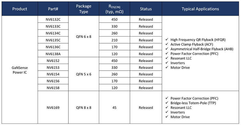
Each of these fault conditions, if left unprotected, can cause thermal overload and damage to the power device. Typical controller over-current or short-circuit protection circuits have inherent delay times that can result in higher maximum current levels than expected. Over-temperature protection circuits typically measure ambient temperatures so it is difficult to correlate to the actual power device junction temperature. By integrating these protection circuits with the power device, the detection-to-protection delay time is greatly reduced to minimize the peak current overshoot, and the maximum junction temperature is more accurately limited. As switching frequencies continue to increase, all of these delay times become even more critical. This further emphasizes the need for ultra-fast detection-to-protection times, and accurate over-temperature control to ensure high robustness for high-frequency and high-density power converter designs. No power transistor other than Navitas GaNSense power ICs has this level of protection with OCP, OTP, and SCP all built-in. The latest GaNSense power IC product line-up (Figure 7) includes a wide range of packages and RDS(ON), suitable to cover a wide range of applications.
Click image to enlarge
Figure 7. GaNSense Power IC portfolio provides solutions for a wide range of power levels and applications