Power module choice impacts system board space and time-to-market
A comparison of alternative on-board power solutions is rarely at the top of the agenda for a board designer. Often designers will use a previous solution because all available resources and time must be spent on the functionality of the system design. However, time spent on the power solution will affect the cost, procurement and sourcing, and will reduce the technical risks and redesign cost. Most importantly it will also have a huge impact and pay-off in terms of reduced time-to-market and increased system packaging density. The main alternatives are standard power modules and discrete power components. Decisions are often based only upon the hardware cost, neglecting many of the other cost elements. A standard power module is a component-like device produced in large quantities, 100% tested and guaranteed to meet the specification in the datasheet. A discrete power circuit consists of many components mounted on the printed circuit board (PCB) together with the main system electronics. There is no testing other than on the finished assembled board. A recent addition to the power module offerings on the market is the PIM (Power Interface Module). An example PIM is shown in Figure 1. A PIM typically contains input filtering and transient suppression, inrush current protection and hot swap functionality, hold-up and under voltage shutdown, dual power feeds, monitoring, alarm and power management based on PMBus or I2C. The first release of a PIM was tailored for ATCA (Advanced Telecommunications Computing Architecture) standard based open platforms to reduce time-to-market and save valuable board space; but the PIM concept and functionality are actually a suitable fit for most boards in information and communications technology (ICT) equipment. Today this functionality is often provided by discrete solutions, but this situation may change due to the shift from proprietary platforms to more flexible and standard-based open platforms. There are a large variety of board-input power interface solutions. Some of them are very simple and contain just a fuse and EMI filtering. Others are more complex and sophisticated, while also including inrush current protection and hot swap functionality, hold-up and under voltage shutdown, dual power feeds, monitoring, alarm, and power management. The power interface circuitry built with discrete components on the board is often a proprietary solution that is adapted for different power system distribution architectures from ICT equipment manufacturers. There are standardization initiatives going on, such as the ATCA, but proprietary solutions are the most common. There are several significant benefits of using a PIM instead of a discrete circuit solution, including reduction of design time and cost, reduction procurement and sourcing cost, reduction of time-to market and reduced board space for the power interface functionality. Circuit and System Design Cost This cost applies only to the discrete power interface circuit; as clearly internal circuit design is not required for the user of standard power modules. The circuit design cost consists of the following items: • Circuit design and layout • Determine component ratings • Specify component part numbers and alternates • Build and test prototypes, including thermal and EMC • Modify circuits as required • Documentation The time and cost will of course differ depending on whether a basic design is already available, or there is a requirement for a completely new design. Design hours spent and hardware cost is a function of the number of components and complexity of the discrete power interface circuit. The result is also dependant on the skill of the electrical designer. In fact, a skilled power design engineer is required to design a robust and cost-effective power interface circuit. However, there will be a power system design cost for both the discrete power interface circuit and for the standard PIM solution. The power system design cost consists of the resources needed and costs for the design of: • DC distribution and decoupling • Thermal analysis and cooling • Safety and fusing • Controls and diagnostics The power system design will be significantly simpler and faster when using the standard PIM alternative, as there are much more advanced built-in functions and support literature available. Procurement and Sourcing Cost This is the resources and direct cost for procuring all of the components required for either solution, including vendor selection and qualification, price negotiation, quality assurance, inventory control, etc. For the standard PIM alternative, there is usually only one component to source, the power interface module. Also, in this case the hours spent and direct cost is a function of the number of components and complexity of the discrete power interface circuit. The discrete power components, as with any other power components, are typically not part of the system board manufacturers' system-functionality electronics bill-of-materials (BOM), and therefore require specific skills and engineers to evaluate, qualify and approve the components and the solution in the specific application. Time-To-Market Cost This extremely important item addresses the technical risk and the fact that the first design is not always the final one. Engineering changes and redesigns are sometimes needed when the solution does not perform as expected. New microprocessors and ASICs are often developed in parallel with the board design with some uncertainty about the final circuit power and supply voltage requirement for the overall system. As the focus is on the performance and functionality of the primary application electronics, the final board power design cannot be finalized until testing and verification of the main system circuitry. This means that there is an apparent risk that the board power and interface circuitry must be re-designed very late in the project, multiplying the design cost and time, causing unexpected delays in the launch and delivery of the new system board. Obviously, there is a larger risk for severe delays when using a discrete power interface solution, as the design is not as well defined or proven and there are dependencies upon several components and vendors. Using a standard PIM solution can make the power system available earlier and thus capture additional sales. The time-to-market cost accounts for the lost revenue (and profit) due to the loss of early product sales if the product introduction is delayed, impacted by the development schedule for the power solution. Not only it is a loss on the number of sold product - but also being early or even better the first on the market may account for a large part of the total revenue and profit as there is less competition and thus a significant higher market price. The time-to-market cost can be a very appreciable number compared with some of the other costs under consideration. With the very short product lifecycles today, this could very well be the determining factor for making a profit or not. PCB Cost The cost of the area on the circuit board occupied by the PIM or the discrete power interface circuit consists of: • Material cost for the PCB itself • Value of the PCB area to the system designer The value to the system board designer will be quite variable. For some systems, with less crowded boards, this cost could be relatively low. For high-density systems with very tight packaging, the system designer may want to minimize the amount of area occupied by power and power interface functions to include additional system application circuitry. In this case, the system board designer and the system manufacturer can assign a higher number to this value, which will serve to impose a cost penalty to the power solutions that have a lower area density. In practice this has become one of the biggest challenges for ICT system manufacturers and system providers. Available space is very limited in all locations and come at a very high cost. Indoor and outdoor applications require minimal floor space and smallest possible equipment dimensions. Another constraint is that modern high-speed electronics require very small distances to minimize distortion by lead inductance and board capacitance. Certain functionality must therefore be built into the same PCB. PCBs are manufactured in certain standardized sizes and the equipment cabinet and shelves are designed for specific board sizes. It is therefore not possible to increase the board size in a given system or equipment building practice. The only solution is to minimize the size and number of components on the PCB. This drives higher integration and smaller and smaller device packages, but at the same time higher functionality requirements result in higher pin count on each microprocessor or ASIC package. The result is very expensive board assemblies, not only because of expensive system electronics, but also due to the extremely high number of board layers required for the functionality. It is not unusual to find up to 30-40 layers in advanced ICT boards. All together this means that board space is very expensive in modern ICT equipment and everything that is not part of the main system electronics needed for the required functionality must be limited to an absolute minimum in terms of board space.
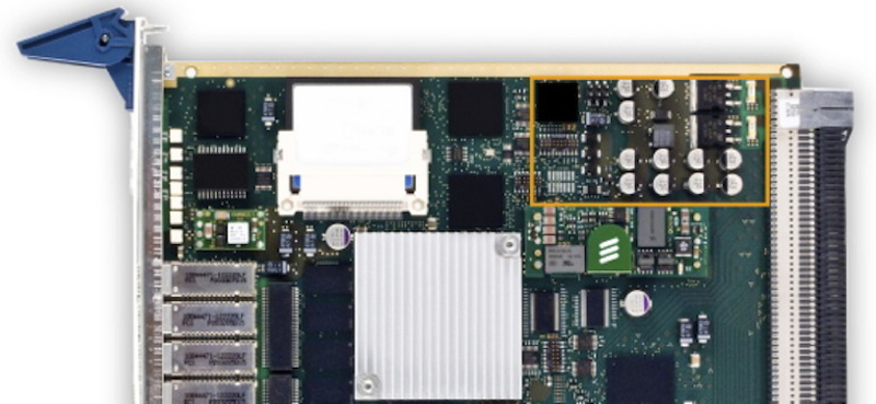
Application Examples The first example is a board with conventional power interface circuitry (see Figure 2). The power interface was designed a long time ago and has been used on many different boards for many years because it works, and besides there is no skilled power design engineer available to improve it. Components are old and costly, and the circuitry occupies a rather large area on the board. There are also increased demands on system availability and requirements for hot-swap and the power interface must therefore be redesigned and include alarm and power management. A PIM will solve all these issues at lower cost and significantly reduced board space.
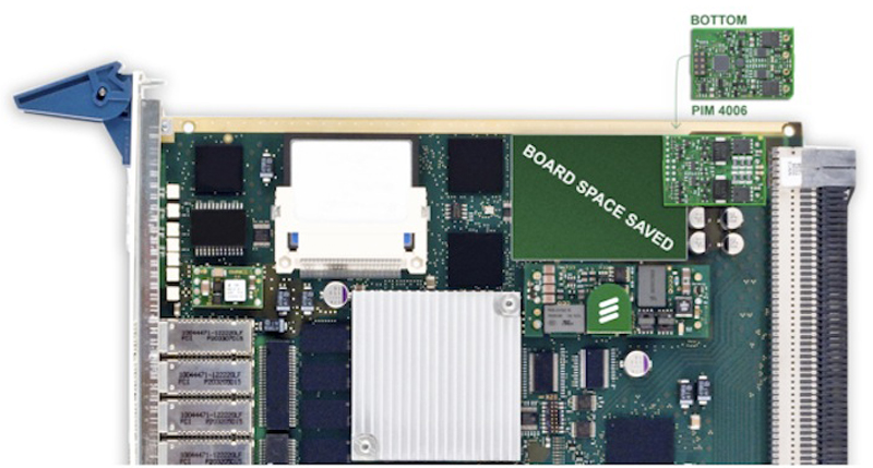
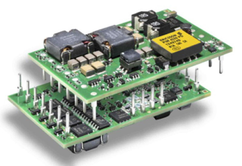
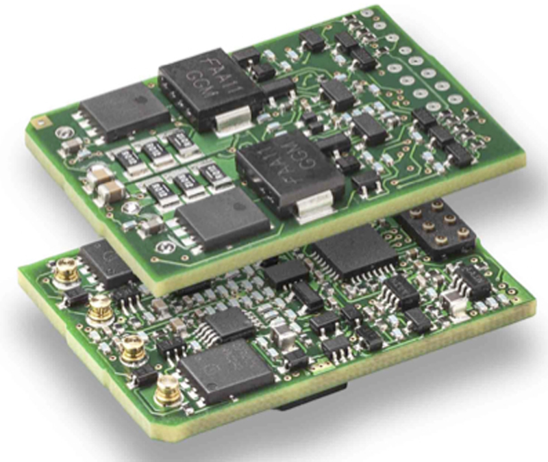
The second example (see Figure 3) illustrates the board space that can be saved using the newly designed sixteenth-brick-format PIM4006 micro-power-interface-module (see Figure 4), which in addition to conventional input circuitry includes an I2C interface.
This module has been developed to meet the highest demands in system availability and robustness and also includes a digital communication interface for system architects to monitor the status of the application via software. The use of the latest technology to increase the amount of filtering has resulted in significant board-space saving (on both sides of the board). This space can be used for additional system processing capability while also simplifying power management and shortening time-to-market. Also in this case, a PIM can save valuable board space and cost. This is possible due to an optimized design made by skilled and experienced power design engineers. The PIM utilizes smaller component packaging and advanced solutions, but still with a reduced bill-of-materials. Power management and internal communication makes it possible to reduce the hold-up time requirement and thereby minimize the required amount of capacitance. The result is a PIM that occupies only one-third maximum of the area taken by the discrete design. Standardization in power distribution for ICT equipment will continue to meet demands from telecom and datacom operators for second sourcing and decreased cost. New PIMs are being developed for different power distribution standards and power levels, as well as proprietary solutions, making them a viable choice in most applications. Ericsson Power Modules