Power Rating extension with 7th generation IGBT and thermal management by newly developed package technologies
Advanced technologies not only for semiconductor devices, but also for packaging
In recent years, significance of semiconductor module for photovoltaic power conversion systems is increasing. Especially higher output power with existing housing size of power module is important to realize further downsizing or rating upgrade for its systems. For realizing higher output, advanced technologies not only for semiconductor devices but also for packaging technologies are necessary because thermal management to handle higher power density of power module is one of the key factors to realize the target. This report is focusing one of the newly developed products family of 7th generation IGBT modules called ‘DualXT’ which housing is widely used in worldwide. Advanced technologies in this paper achieve over 30% upgrading of current rating of the product which can create significant benefit for powerconversion systems.
Introduction
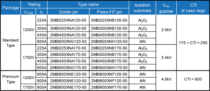
Table.1 shows newly developed 7th generation Dual XT families. 7th generation Dual XT have 2 kinds of package which are ‘Premium type’ and ‘Standard type’. Premium type has properties of 4k VAC isolation voltage guarantee and high CTI reign case (CTI > 600). Recently, demand of NPC (Neutral Point Clamped) topology for 3 level solution is increasing. Especially 1500 VDC by it topology is highlighted at solar conversion application to realize high efficiency. Premium type DualXT has been developed as suitable device for the usage.
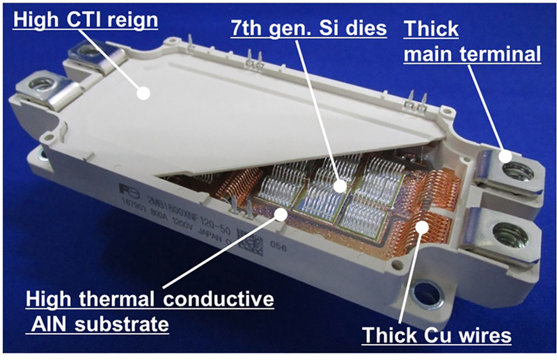
Furthermore, the maximum current rating of the products is 800A which is 33% upgrade against conventional600A.To realize the upgrading, many advanced technologies are applied such as IGBT and FWD performance improvement which is main stream of IGBT module supplier’s trend. However, the significant upgrading cannot be achieved only the device improvement because of its high density of power dissipation. Therefore, further thermal management for Si dies is necessary. Moreover, package current limit is also one of the subjects of this paper,because small package and higher current combination causes high temperature rise inner and outer of electrical circuit connections which have to be overcome. Therefore the 7th generation Dual XT has many well-considered features in Fig.1, such as power dissipation improvement by newly developed 7th generation IGBT and FWD Si dies, lower thermal resistance by high thermal conductive thinner AlN ceramics, temperature reduction at internal electrical wiring connection and main terminals by optimized internal circuit layout and Cu wire, thicker main terminals. These advanced technologies combination can realize 49% higher output in real application usage in Fig.10.
Click image to enlarge
Fig.1 Features of 7th generation Dual XT
Click image to enlarge
Table. 1 7th generation Dual XT families
7th generation IGBT and FWD technologies
In order to improve the efficiency of energy conversion, it is necessary to improve power dissipation for IGBTmodules,and the characteristics of this power dissipation depend on the properties of the semiconductor chips of the IGBT or and Freewheeling diode(FWD).
Dual XT has 2 kinds of voltage rating which are 1200V and 1700V. Both rating of IGBT and FWDare developed based on same technologies[1] [2].
IGBT characteristicimprovement
Improvement of collector-emitter saturation voltage has been realized by reducing the thickness of the drift layer in the 7th generation Dual XTIGBT. Furthermore, the voltage oscillation and withstand voltage degradation that can occur in the case of thinned drift layers during turn-off has been suppressed by optimizing the field stop (FS)layer.
The trade-off relationship between on-state voltage drop and turn-off energy is shown inFig.2. On-state voltage drop was reduced by 0.4V and turn-offenergyreductionofapproximately 7% from the 6th generation DualXT.
FWD characteristic improvement
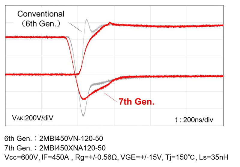
Reduction of the anode-cathode forward voltage has been realized by reducing the thickness ofthe drift layer in the 7th generation Dual XT FWD. In addition, Softer reverse recovery waveforms compared with conventional product has been achieved by optimized local life time control as shown inFig.3.
Furthermore, significantly reduced reverse recovery energy by reducing reverse recovery peak current and tail current has been realized.
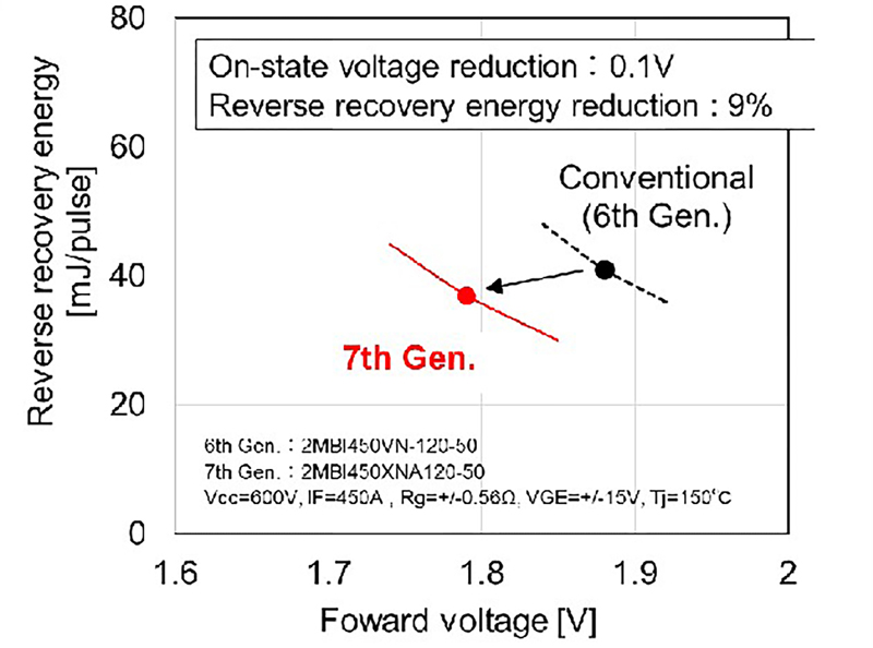
The trade-off relationship between on-state voltage and reverse recovery energy is shown in Fig.4. On-state voltage drop was reduced by 0.1V and reverse recovery energy reduction of approximately 9% from the 6th generationDualXT.
Power dissipationcomparison
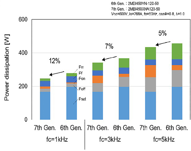
The result of calculating power dissipation is shown in Fig.5. As a result of the improvements mentioned in Sections 2.1 and 2.2, the X Series Dual XT has been able to reduce powerdissipation by approximately 12% at carrier frequency of 1kHz when compared with conventional products.
.jpg)
Click image to enlarge
Fig.2 Turn-off energy vs. VCE(sat)
Click image to enlarge
Fig.3 Reverse recovery waveforms
Click image to enlarge
Fig.4 Reverse recovery energy vs. VF
Click image to enlarge
Fig.5 Comparison of power dissipation
7th generation Dual XTpackage technologies
The power dissipation improvement ratio is 5~12% by advanced Si dies technologies. However, high power output more than 130% cannot be realized by only the technologies because of its higher power dissipation density which causes higher temperature rise of Si dies. In addition, thermal management of electrical connection is also key factor for the upgrading as already mentioned in above. 7th generation Dual XT realizes the target by combination of the Si dies and new package technologies which are introduced in this section.
Thermal conduction improvement by new thinner AlN substrate
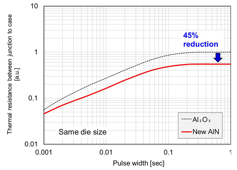
In order to improve the heat dissipation from the chip, the 7th generation IGBT modules use insulated substrates with highly improved thermal resistance. The insulated substrate has the highest influence on the total thermal performance of the module. Standard materials widely used as insulated substrate are inexpensive Al2O3 substrate and high thermal conductivity AlN. Since such low thermal resistance is necessary there is no way around the high performance AlN. Furthermore, the thickness of the AlN substrate needs to be reduced in order to improve the thermal resistance and long-term reliability. By enhancing the material bending strength of the AlN substrate a thinner substrate compared to conventional AlN can be realized. The thinner substrate achieves better thermal cycling capabilities by relaxation of thermal stress and greater heat dissipation compared toconventional AlN substrate [3]. Finally the thermal resistance of the IGBT modules was greatly reduced and heat dissipation and reliability was increased by applying this new AlN substrate. The thermal resistance of new AlN substrate between junction to case is shown in Fig.6. Comparing to generally used Al2O3 substrate, the thermal resistance of new AlN substrate was reduced by 45%. By applying the new AlN substrate in the 7th generation Dual XT, temperature rise due to the shrinking of the chip size was successfully solved.
Click image to enlarge
Fig.6 Comparison of the thermal resistance between junction and case at same die size.
Thermal management of electrical connections
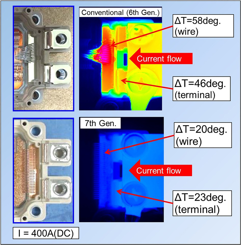
As already mentioned, package current rating had limitationforupgradingofoutputpower.Thebottle neck of conventional package is temperature rise at output terminals and internal Al wire electrical connections. For counter measure, thicker diameter Cu wire is adapted for 7th generation Dual XT package with optimized internal layout to realize better current balance between the wires. More than 30% thicker main terminals are also adapted. Fig.7 shows thermal experimental evaluation results of new and conventional Dual XT. More than 50% of temperature rise deduction for both internal wiring and main terminal are realized with 7th generation Dual XT package.
Click image to enlarge
Fig.7 Terminal and wire temperature comparison
Expansion of continuous operation junction temperatureTjop
In order to achieve an even higher output current for the 7th generation Dual XT, the continuous operation junction temperature Tjop has been expanded from 150°C to 175°C compared with conventional Dual XT. To expand Tjop, it was necessary to improve delta Tj power cycling capability, while also enhancing long-term reliability at high temperatures.
The delta Tj power cycle capability is shown in Fig. 8. In conventional products, there would be a dramatic degradation of the delta Tj power cycle capability when Tjmax = 150°C to 175°C. In the 7th generation Dual XT, however, the application ofanewlydevelopedsoldermaterial[1] and the use of a new wire bonding technology for the semiconductor chip have enabled a capability that is approximately twice that of conventional products under conditions of Tjmax=175°C,dTj= 50°C. As a result, the delta Tj power cycle of the 7th generation Dual XT has higher capability at Tjmax = 175°C that exceeds conventional products operating at Tjmax =150°C.
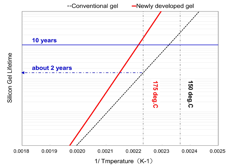
Then, relationship between temperature and life time of the silicone gel is shown in Fig.9.
For the long term reliability of 7th generation Dual XT, the deterioration of silicone gel at higher operating temperature must be improved for expansion of Tjop. Conventional silicone gel has life time of ten years or more at a temperature of 150°C, but it degrades to approximately two years at temperature of 175°C. The newly developed silicone gel [1] has life expectancy of ten years or more even at a temperature of 175°C, which can be realized same life time of the silicone gel of conventional products operating at 150°C.
Click image to enlarge
Fig.8 dTj power cycling capability curve

Click image to enlarge
Fig.9 Temperature dependence of silicone gel lifetime
Conclusion
The 7th generation Dual XT has reduced power dissipation through enhancing characteristics of semiconductor chip, and also improving current carrying capability for package by improving package structure. Furthermore, it has achieved continuousoperationatTjop=175°Cbyimproving delta Tj power cycle capability and longer life time of newly developed siliconegel.
As the results, it is capable of improving output current during actual operation and energy conversion efficiency in products utilizing IGBT modules such as inverters.
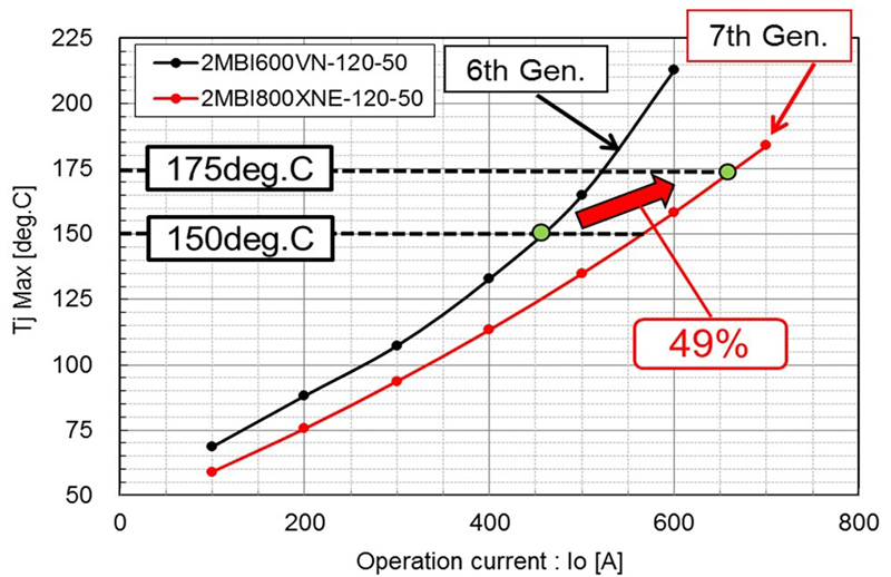
As an example of the effect of these enhancements, relationship between inverter output current and IGBT junction temperature is shown in Fig.10. By applying the 7th generation Dual XT, output current can be increased by 49% compared with conventional products
Click image to enlarge
Fig.10 Upgrading of output current
Fuji Electric