This article continues the series in which Dr. Ridley documents the processes involved in taking a power supply from the initial design to the full-power prototype. The second layout of the PC board incorporates significant changes in the power stage, changing the number of outputs from three to five. Some of the issues involved in the coupled-inductor magnetics design are discussed.
Three Output Coupled-Inductor Design
The original specification for the power supply design was as follows:
1. Output 1 – 35 VDC @ 10A isolated
2. Output 2 – 35 VDC @ 10 A isolated
3. Output 3 – 15 VDC Bias power and regulated output, primary referenced
4. Maximum power 350 W (only one output fully loaded at a time, application is for audio.)
5. Input – 180 – 265 AC
6. Power Topology: Two-switch forward
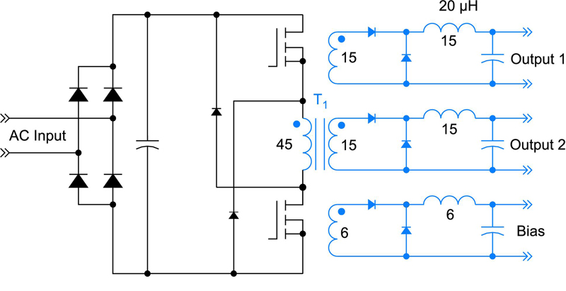
Figure 1 shows the schematic of the three-output forward converter. A single core inductor is used with three windings, one for each of the outputs. This coupled-inductor approach provides the best cross-regulation between each of the outputs. There are two major advantages of coupled inductors – firstly, all of the outputs are tied together through the transformer action of the inductor, preventing them from having individual resonant frequencies. Secondly, regardless of individual loading on each of the outputs, the coupled inductor forces all of the outputs to be in either continuous or discontinuous mode concurrently, greatly improving the regulation.
As shown in an earlier part of this series, excellent regulation was achieved with a wide variation of output loading.
Click image to enlarge
Figure 1: Forward Converter with Three Coupled-Inductor Outputs
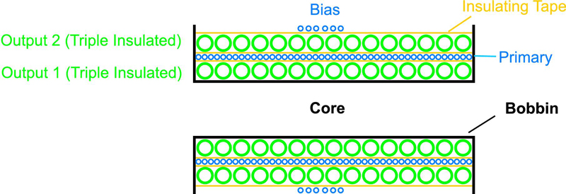
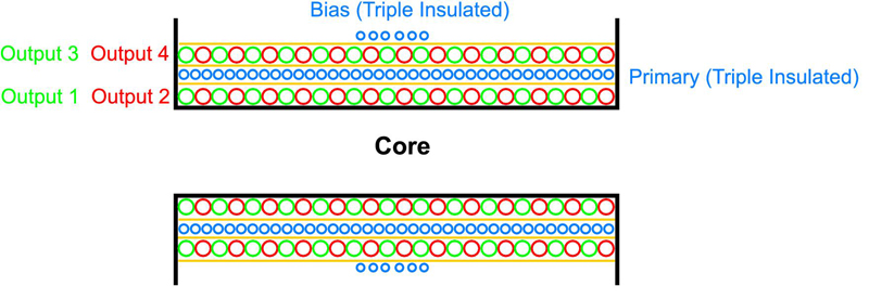
Figure 2 shows the winding layout for the three-output transformer. The first layer of winding was the first secondary output, consisting of 15 turns wound with triple-insulated kapton wire. This winding used a single strand of wire, with a gauge selected to exactly fill one layer of the bobbin. One layer of magnetics tape was added on top of this secondary to provide a smooth winding surface for the subsequent windings.
The next layer of winding is a single layer primary with 45 turns of magnet wire, followed by a layer of tape. The third layer is the other high-power secondary, followed by 6 turns on the final layer for the bias supply and regulation winding. For coupled designs, the lowest power winding is placed on the outside of the winding sequence for best cross-regulation.
Click image to enlarge
Figure 2: Three-Output Transformer Winding Layout
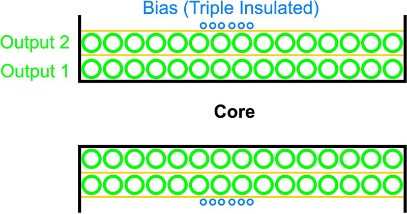
Figure 3 shows the winding layout of the coupled inductor. Notice from the schematic of Figure 1 that the turns ratios of the inductor and transformer are critical, and the ratio between the different secondaries must match exactly. Hence the transformer has a ratio of 15:15:6 for the secondaries, and this exactly matches the turns count for the inductor. Apart from this caution, the design of a coupled inductor is not particularly difficult. The simplest approach is to design the inductor as though it were a single-output design rated at the power of the sum of the three outputs. This sets the required number of turns for the inductor value required with the selected core area.
Click image to enlarge
Figure 3: Three-Output Coupled-Inductor Winding Layout
The layout of the inductor in this case is the same as the transformer, starting with each of the high power secondaries, and finishing with the bias winding. Notice that the bias winding, which is primary referenced, is the one with the triple-insulated kapton wire. This reduces cost of materials and processing time during the inductor construction.
Five-Output Coupled-Inductor Design
The original plan for this project was to provide two main power outputs, and one regulation winding. A second power supply was to be used to provide the exact same outputs to a second load amplifier of a stereo pair.
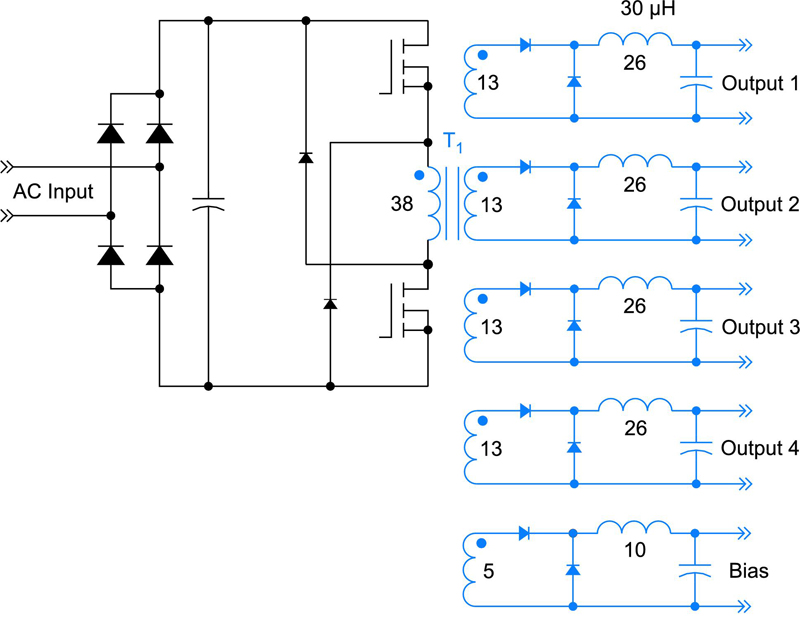
However, during system testing, it became clear that the final load was less than expected, and that all four outputs could possibly be provided with a single power stage. A decision was made during the second board layout to incorporate this change into the design, providing five outputs from a single forward converter. The schematic of the five-output converter is shown in Figure 4.
Click image to enlarge
Figure 4: Redesigned Forward Converter with Five Coupled-Inductor Outputs
This is a significant change to the project, but one which provides substantial savings in parts, board area, and cost. The risk is in whether the tight cross-regulation is lost with more outputs. The new design also presents something of a technical challenge during the board layout. One of the significant complications of coupled-inductor designs is managing the multiple connections of the transformer, the inductor, and the rectifier diodes on the printed circuit board.
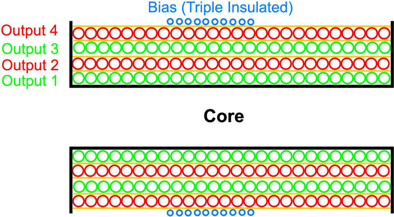
The extra outputs also present significant changes to the transformer and inductor designs. There are now a total of six windings in the transformer, and changes must be made to accommodate the extra complexity. Figure 5 shows the winding layout of the transformer. The first two secondaries are wound bifilar with each other to exactly fill the layer with 13 turns on each secondary of magnet wire.
The turns count was reduced because the primary layer could no longer accommodate the same 45 turns as before in the bobbin. With more secondaries, it made better manufacturing sense to use triple-insulated wire for the primary rather than the secondaries. Only 38 turns could fit in the layer neatly. This reduced turns count raises the core excitation, and the switching frequency must also be raised slightly to 250 kHz from 200 kHz in order to avoid saturation of the transformer.
After the primary is wound, the remaining two secondaries are placed on top of this, wound bifilar with each other. Five turns of the bias winding complete the transformer design.
Click image to enlarge
Figure 5: Five-Output Transformer Winding Layout
The secondary turns ratio of the transformer is now 13:13:5, and this ratio must be maintained exactly in the inductor. For the previous inductor design, 15 turns were used in the inductor main outputs, but this pushed the design hard in terms of flux level, and only 20 µH inductance could be used, resulting in significant output ripple.
With the reduced power requirements observed in the system testing, a decision was made to raise the turns count on the main output to 26. This allowed a larger inductance of 30 µH with a reduced core flux level. The value of 26 was chosen since it allows us to exactly the match the transformer turns ratio when 10 turns are placed on the bias winding of the inductor. Normally for a forward converter inductor, the value of inductance and the number of turns are determined by the current level and core area. In the case of the coupled inductor design, however, maintaining the proper turns ratio is paramount, and the number of turns is set by this requirement. This allows the value of inductance to be increased as a consequence.
It must be remembered that in magnetics design, we have many degrees of freedom, and there are no hard rules determining the value of an output inductor. It is important not to overconstrain thinking, a common error of many design books on magnetics. For example, many texts will fix the value of inductance to give a specified ripple current, but this removes freedom for the designer to choose a value that, in reality, can be varied over a significant range without detriment to the overall performance.
The layout of the new inductor is shown in Figure 6. Each winding occupies a single layer of the inductor, with the wire gauge choses to exactly fill the layer neatly. The final layer is the 10 turns of bias winding, using triple insulated wire.
Click image
Figure 6: Five-Output Coupled-Inductor Winding Layout
Summary
The turn of a PC board is usually a major project milestone. It presents the opportunity to clean up previous errors in a board, improve manufacturability, and move a step further towards a final product.
However, in many projects, the PC board iteration is often seen as an opportunity to revisit project goals, and make major changes to a design project and its specifications. In this particular project, a large number of changes have been made, and the risk of incorporating these changes has to be balanced against the potential gains in the final product. The risk here is not too great since there is always the option of reverting back to the previous design of just three outputs if the regulation achieved during testing is insufficient.
It must be stated, however, that substantial changes to components, especially the magnetics, will result in the need to reiterate much of the testing of the power supply, and the time to do this must not be underestimated. The changed turns of the transformer and inductor will affect the cross-regulation, EMI, ringing, snubbers, current protection, and semiconductor stresses.
If the second iteration had been undertaken with none of these changes, and the design remained unchanged with three outputs, there is a reasonable expectation that this would be the final PC layout before production. However, the substantial changes make it likely that a third layout pass will be needed before finishing the design.