High Efficiency Power Distribution and Charge Pump Solutions for Robotic Hands
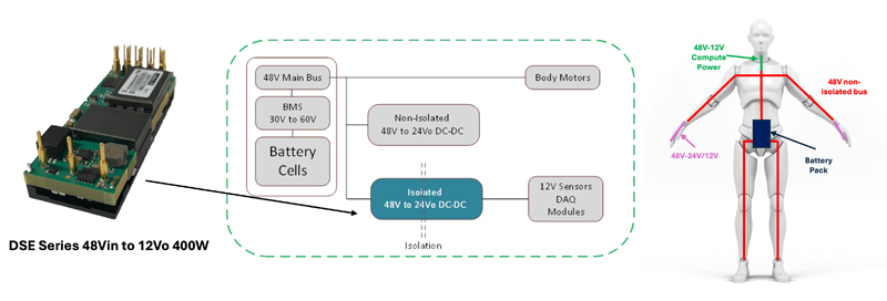
Figure 1: Non-isolated bus distribution – 48V bus is unregulated and not isolated
As humanoid and physical‑AI robots become more capable and dexterous, efficient and reliable power delivery has emerged as a critical design challenge. This article explores modern robotic power distribution architectures and examines how advanced charge pump–based converters enable compact, high‑efficiency power solutions for space‑ and thermally‑constrained subsystems, such as the dexterous robotic hand.
Robotics power distribution chains
Robotic power distribution architectures continue to evolve to achieve the best balance of efficiency, power dissipation, thermal performance, safety, and system cost.
Two primary power distribution architectures are emerging in humanoid robotics applications.
The first distributes power directly from a battery‑derived 48V rail as a non‑isolated system bus shown in Figure 1. While straightforward, this approach introduces several challenges. The bus voltage varies widely—from deeply discharged to fully charged battery levels—and is further stressed by voltage transients generated by the high-power motors supporting the major joints of the humanoid. As a result, the bus often exceeds Safety Extra Low Voltage (SELV) safety limits, requiring the use of downstream isolated converters, such as the Murata DSE 48V series, or more complex downstream insulation and isolation strategies combined with high-voltage non-isolated converters.
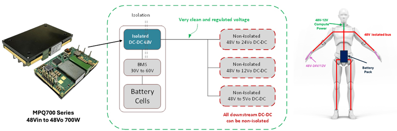
Figure 2 shows an alternative approach which generates an isolated, regulated system bus using a high‑efficiency isolated power converter, such as the Murata MPQ700 quarter brick series – capable of supporting 700W with an input voltage range of 36-75V. This architecture simplifies the overall safety strategy by allowing downstream converters to remain non‑isolated, while also delivering a clean, low‑noise, and tightly regulated bus. The improved power quality benefits EMI performance and helps to ensure robust, error‑free data communication across the robot.
Click image to enlarge
Figure 2: Isolated bus distribution – stable and clean, isolated 48V bus
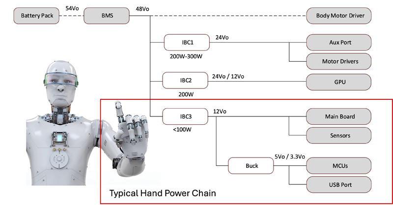
Figure 3 shows a generic power train for a humanoid robot which assumes the use of an isolated distribution architecture and the availability of a regulated 48V bus, which can then be converted to lower voltages supporting the joint motors, sensors, and control systems.
Click image to enlarge
Figure 3: Humanoid robot – typical power train using a regulated, isolated 48V bus
The more traditional method of converting from 48V to the load would be to use a buck switching regulator. Given that the input is regulated to 48V, we can employ charge pump, switch-capacitor technology. This improves efficiency and power loss, and enables lower-profile compact footprint and reduced weight by eliminating the large output inductor. As Figure 3 shows, charge pumps can be used in various areas in the humanoid power chain, including on-board compute and data acquisition. However, this paper focuses on charge pumps for the dexterous hand where the need for size and weight is at a premium.
The dexterous hand – power delivery
The dexterous robotic hand represents one of the most complex and technically demanding elements in physical AI and humanoid robotics systems. The humanoid-style hand must simultaneously achieve fine manipulation, strength, responsiveness, and safety within a highly constrained form factor. The primary challenge arises from the hand’s high number of degrees of freedom. A human hand contains approximately 20–27 degrees of freedom, depending on joint definition, allowing for a vast range of coordinated motions and dexterous tasks. Replicating this capability requires a dense network of joints, tendons, and actuators packed into the limited volume of human-sized fingers and palm.
Power delivery and thermal management pose critical constraints. Fine motor control typically requires continuous actuation, meaning that many robotic hands consume significant energy even when holding objects statically. Packing multiple motors and drive electronics into small fingers creates extremely high power-density environments, making heat dissipation difficult. In short, power delivery to the hand and joint area must be high efficiency with minimal power dissipation, compact size, and low-profile to fit within the forearm area. Additionally, power conversion devices must be shock and vibration proofed. Large magnetic inductor components are vulnerable to damage during rigorous activity.
The lower section of Figure 3 shows a typical humanoid hand power delivery chain. Typically, the isolated 48V would be routed directly to the larger more powerful motors, usually a permanent magnet synchronous motor, in the shoulder, elbow, hips, knees, and ankles. As an illustration, the shoulder would typically draw around 500W continuous with up to 1200W peak for short durations. Similarly, the elbow would draw around 200W continuous with up to 500W peak. So, there is a significant amount of power dissipation in the humanoid arm, even at rest.
The wrist and hand joints are more likely to use miniaturized brushless DC permanent magnet motors supplied from a lower input voltage, 12V or 24V. Typically, the wrist would be around 200W continuous power consumption with transients around 400W, while the hand would typically be 100W continuous with 200W power peaks.
Why not a buck converter?
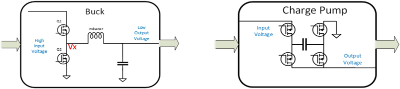
High‑efficiency conversion from the 48 V system bus to 24V or 12V is therefore essential. One approach is to use a traditional buck switching regulator (Figure 4a). However, this method presents several disadvantages in space‑constrained robotic hands:
· Lower efficiency and higher power dissipation, particularly if space and height are limited.
· Large output inductor, if it fits in the space. Care is required to mount and secure the inductor to prevent mechanical shock and damage.
· Electromagnetic interference (EMI) with surrounding electronics, particularly high-speed data communication paths.
The EMI can be significantly worse in higher voltage buck converters as the Vx node (Figure 4a) swings between VIN (48 VIN) and ground. However, the actual voltage spike at Vx is much higher due to the reverse leakage of the inductor and board parasitics, often closer to 100V peak.
Click image to enlarge
Figure 4: (a) Traditional buck converter (b) Charge pump, switching capacitor divider
Charge pump, switching capacitor dividers
An alternative to the buck converter is the charge pump, also known as a switched‑capacitor divider (Figure 4b). Although inherently open‑loop and unregulated, charge pumps provide extremely high efficiency and are well suited to low‑profile designs. When the 48V input bus is fixed or pre‑regulated, the lack of regulation is not a limitation.
A charge pump (CP) is a type of DC-DC converter that stores and transfers energy through switched capacitors (SCs), effectively increasing or lowering a DC voltage. It is an alternative to inductor-based converters and is commonly employed in high conversion ratio applications that require improved efficiency and a low-profile format. Without the large output inductor, a charge pump can be an ideal solution for space challenged and low-profile solutions.
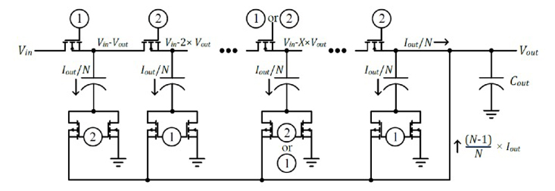
Figure 5 shows a simplified divide‑by‑N Dickson charge pump. As the voltage‑division ratio increases, the number of stages increases linearly, while the current through each stage decreases proportionally. Importantly, each switch is exposed to a maximum voltage of only 2 × VOUT, regardless of the division ratio. This allows gate‑charge losses to remain essentially constant as the conversion ratio increases.
Click image to enlarge
Figure 5: Divide-by-N Dickson charge pump
The Dickson charge pump places the burden of withstanding high voltages on the capacitors, not the switches. In contrast, a typical series-parallel charge pump (the most common architecture) drops the high voltage on the switches rather than on the capacitors. The gate-charge losses in this architecture increase with VIN because the gate capacitance of the switches increases with the voltage rating. In addition, the series-parallel architecture design cannot be extended to a multi-phase configuration.
Figure 6 shows a Dickson divide-by-2 charge pump with a single capacitor and four switches. This circuit works in two states:
· In state 1, Q1 and Q3 are closed, but Q2 and Q4 are open. In this state, the positive and negative terminals of C1 are connected to VIN and VOUT, respectively. The VIN is reduced by the charge stored on C1 and it is balanced by the output capacitor (COUT).
· In state 2, Q1 and Q3 are open, but Q2 and Q4 are closed. The negative terminal of C1 is connected to ground, and the positive terminal is connected to COUT. Because the voltage across a capacitor cannot change instantly, it attempts to maintain an equivalent balanced voltage, where VOUT is the divide-by-2 of VIN if C1 and COUT are equal.
Click image to enlarge
Divide-by-2 charge pump State 1. C1 is charging State 2. C1 is discharging
(a) (b) (c)
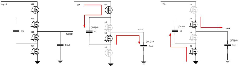
Figure 6: Divide-by-2 Dickson charge pump (a) and its switching states (b and c)
Adding adiabatic or lossless energy transfer
pSemi’s adiabatic or lossless soft‑switching charge‑pump architecture reduces switching losses by temporarily storing charge‑redistribution energy in a small inductor and recycling it back to the output. This approach improves efficiency and significantly reduces EMI compared with conventional charge‑pump implementations.
The charge redistribution losses are caused by the voltage differences in the capacitors while charging and discharging the stored energy. In a charge pump, a capacitor is typically switched in parallel or in series with other capacitors resulting in charge redistribution loss. This redistribution loss is a function of capacitor size and switching frequency.
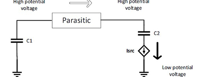
If C1 and C2 are identical capacitors, and C1 is charged to higher voltage than C2, the starting energy is twice the ending energy after the charge redistributes and balances. The lost energy is dropped across any parasitic components in the current loop. Because the charge is moving from high-to-low potential, power is lost. As more of the charge moves from C1 to C2, the voltage on C1 drops and the voltage on C2 rises. This reduces the voltage potential across which the charge needs to move and thus reduces energy loss. In other words, energy loss is reduced as the voltage potential between the two capacitors equalizes.
pSemi has developed charge pump architectures that use a small, adiabatic output inductance. Adding an adiabatic inductor allows the current to resonate between capacitors and eliminates the charge redistribution losses in the fly capacitors. The simplified block diagram in Figure 7 shows that the voltage drop occurs at the current source (ISRC) and the energy is absorbed inside the current source like an inductor and recycled to the output load.
Click image to enlarge
Figure 7: Charge pump redistribution power loss with current source
Practical implementations
This section focuses on practical implementations of charge pump, switching capacitor divider conversion from a regulated 48V bus to the robotic hand, where 24V or 12V is required to provide power to the motors, sensors, and controls.
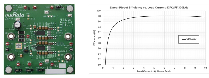
The implementation in Figure 8 uses the PE25208 charge pump IC in divide-by-2 mode to generate 24V. The PE25208 can be configured for divide-by-2 or divide-by-3, if a lower output voltage is required. In the case below, two devices are connected in parallel to deliver over 240W (24V @ 10A) with efficiency around 98%. The low power dissipation means that minimal heatsinking or cooling is required. The key advantage of the design in Figure 8 is the small solution footprint (15.5 mm × 30.8 mm) and the low-profile of 2.7 mm height. This can be further reduced by around 20% with a 1 mm top-side component height by placing components on both sides of the board. There is no large output inductor as in a traditional buck converter. The PE25208 solution uses a small chip-inductor for adiabatic or lossless switching for efficiency and EMI improvement.
Click image to enlarge
Figure 8 – Two PE25208 modules connected in parallel with efficiency data recorded at 48VIN
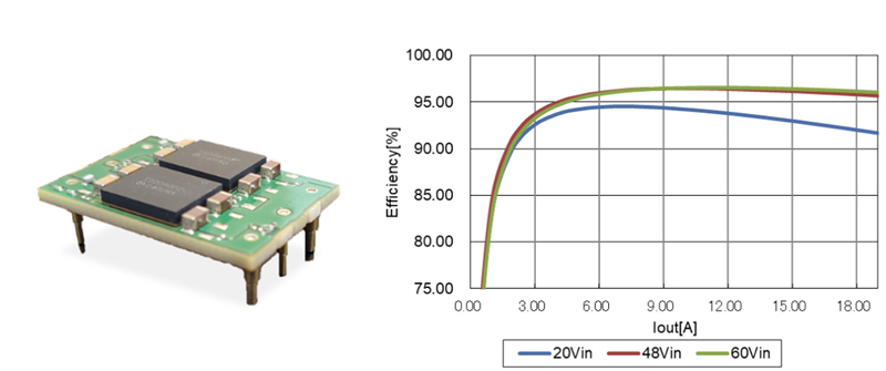
The PE25304 is a charge pump module with all external passive devices included in the same LGA package (11.5 × 9.5 × 2.1 mm). The PE25304 has an input range of 20V to 60V and can deliver 6A @ 12V output from a single device. In the Figure 9 example, two PE25304 modules are connected in parallel to deliver around 140W of power. In this example, the two PE25304 modules are placed on a carrier board with the dimensions and pinout of a traditional 1/16th brick module. Hence, the assembly can be used to replace other 1/16th brick modules. Like the PE25208, no large output inductor is required, which makes the solution less vulnerable to shock, vibration, and movement of the robotic hand. The efficiency shown in Figure 9 peaks at around 97% at 10-12A (around 140W).
Click image to enlarge
Figure 9: Two PE25304 modules connected in parallel capable of delivering 140W at around 97% efficiency
Both charge pump solutions using a PE25208 divide-by-2 module and a PE25304 divide-by-4 module provide high efficiency, low power loss solutions ideal for low-profile and space-constrained areas, such as the robotic hand power delivery.
Summary and conclusions
The increasing power density and functional complexity of humanoid robots means that power delivery architectures continue to evolve to find the optimal balance of power, efficiency, size, and weight. In particular, the humanoid dexterous hand requires high power delivery in an already congested area.
Advanced charge pump, switching‑capacitor converters—especially those incorporating adiabatic energy recycling—offer a highly efficient, compact, and mechanically robust alternative to conventional buck regulators for fixed‑ratio voltage conversion. By eliminating large inductors, these solutions reduce EMI, improve shock and vibration resilience, and enable ultra‑low‑profile designs without sacrificing power capability.
As humanoid robots move closer to large‑scale deployment in real‑world environments, charge pump–based power conversion represents a key enabling technology, helping designers meet the demanding efficiency, size, weight, and reliability requirements of next‑generation robotic systems.


