Probing Tips for High-Performance, Low-Power Circuits
Low-power circuits combine high speed and low-power consumption in a single component, presenting a number of probing and testing challenges. Since many low-power devices are also high-speed systems, there is a need to test and verify their performance. Testing the low-power components for compliance with industry standards is often required to ensure interoperability between components or systems. In addition, testing a design ensures its reliability in use and across multiple manufacturing lots. Typical tests performed include voltage and timing measurements, including jitter and noise measurements. The most common tool for these tests is the oscilloscope. While connecting to the low-power device under test might be possible with a coaxial cable, many systems require an oscilloscope probe to acquire the signals.
Low-power devices use a variety of techniques to reduce power consumption. One simple method is to reduce the power supply voltages and the peak-to-peak voltage swing of high-speed signals. Another technique is to switch the circuits’ operating mode between a high-speed state and low-power states. The lower-power states may include a standby mode or they may involve the system running at a reduced data rate. A third technique to reduce power consumption is to use shorter interconnects with reduced capacitance. These shorter interconnects in mobile devices consume less power than longer interconnects found in large computer systems.
When low-power components change state to a low-power mode they will often be in a high-impedance state. Some systems even run without termination to conserve power. For example, the MIPI D-PHY bus operates in an unterminated state when it is communicating in its low power, low data rate state.
Others return to a standby voltage level when the bus is un-driven. This state may be accomplished using a large, weak pull-up resistor to the standby level. LPDDR2 and LPDDR3 both use this method that allows the bus to float to the tri-state level when the bus is not being actively driven.
In general, the oscilloscope probe needs to present a higher impedance input than the characteristic impedance of the circuit to prevent loading. Otherwise, the probe can load down the circuit or cause unwanted distortion of data signals. With the low-power circuit running in a high-impedance state, the impedance of the probe needs to be as high as possible.
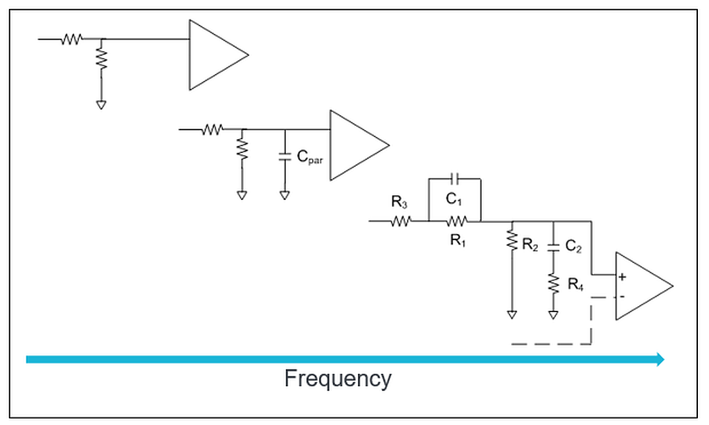
There are many probes available with high input impedance at low frequencies (DC-100Hz). At these frequencies, the impedance of typical probes looks like a large resistor as shown in the top left of Figure 1. Typical impedance specifications at low frequencies range from 40 kΩ to 1 MΩ. As the frequency of the signal being measured increases, the parasitic elements that make up the probe tip and probe amplifier can look like capacitors such as that shown in the middle of Figure 1. The most desirable probes like that shown in the lower right of Figure 1 have high frequency performance as well as high dynamic range. Extending the frequency and voltage range of a probe requires a front-end network of resistors and capacitors. However, adding capacitance to the front-end can result in a lower input impedance at high frequencies.
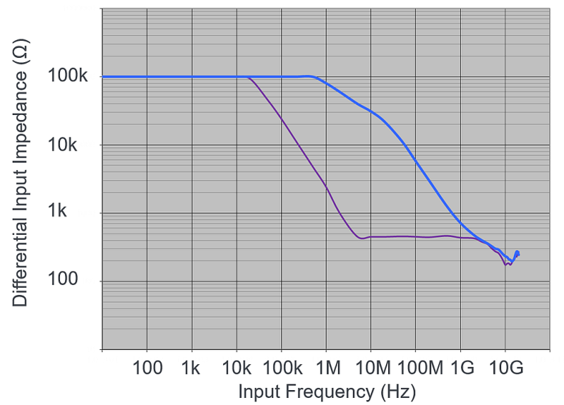
The purple trace in Figure 2 shows the impedance of a high bandwidth probe vs. the input frequency of the signal. The probe’s impedance starts out high, but drops as the signal’s frequency increases. This probe has an impedance of roughly 500Ω for signal frequencies below 2 GHz. Ultimately at very high frequency, even small features of the probe become capacitive and the impedance drops again. Stray inductance in the probe’s inputs can also cause the input impedance to increase slightly.
Click image to enlarge
Figure 2. A higher performance probe (blue trace) offers higher impedance as input frequency increases.
Fortunately, there are higher performance probes on the market with higher impedance characteristics that are able to maintain high input impedance at high frequencies while providing high signal fidelity. Such a probe is shown by the blue trace in Figure 2. Notice that the impedance of higher performance probe is much higher in the frequency range from 1 MHz to 1 GHz. This difference in impedance can make a significant impact in reducing the loading on a low power circuit.
Signal Access Challenges
Another challenge for many applications is probing in systems with tight areas where there is limited access to test points. Many times, test points are within a chassis, located between circuit boards or under heat sinks, or are simply fine pitch pins and vias. Also in an effort to save power, the lengths of the system’s interconnects are kept to a minimum.
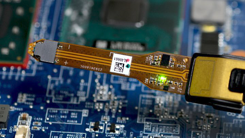
To address these challenges, the latest probes use a very small probe head connector combined with a flexible probe cable along with solder tips to connect to the device under test (Figure 3). These solder tips are also very thin and narrow and are flexible enough to route around many of the obstacles that are likely to be encountered on a system. To protect the delicate solder connections on a device under test, solder tips can also be strain relieved using tape, glue, or other common strain relief materials. To make this easier, some probe manufacturers offer tips that are flat on one side so they can lay flat on many surfaces and adhere well to tape and glue.
Click image to enlarge
Figure 3. Here is a solder down, flex circuit accessory for the Tektronix P7700 Series TriMode probe with an active buffer amplifier on its tip. This system provides up to 20 GHz bandwidth and enables probe access in tight areas.
Noise Challenges
The final challenge for testing low-power circuits is the low amplitude of their high-speed signals. By reducing their signal swing, low- power components reduce power consumption. Some examples of these low signal swings include MIPI D-PHY in high speed mode (140-520mVpp), MIPI M-PHY small amplitude (SA) (160-400mVpp) and LPDDR4 (400-480mVpp).
Accurately measuring these low voltage signals requires high sensitivity and high bandwidth in the scope and probe. High impedance probes attenuate the acquired signal in order to acquire signals with a wide dynamic range. The disadvantage of attenuation in the probe is that it acts as a noise multiplier for the measurement system. While many probes have a 10X attenuation value, it is best to use a probe with a lower attenuation setting to minimize the additive noise of the probe.
Click image to enlarge
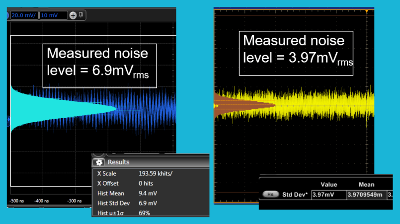
Figure 4. Probe noise can vary significantly across scope and probe combinations. Noise can be a critical barrier when trying to measure low amplitude signals that have been further attenuated by other losses.
Figure 4 compares baseline noise of two different probe and scope combinations from different vendors when they are set to their maximum sensitivity and minimum attenuation. Notice that some probes and scopes show large amount of noise, taking up multiple on-screen divisions, when they are set to maximum sensitivity. The maximum sensitivity setting can be important if you are trying to measure a low amplitude signal that has been further attenuated by losses on the board or through connectors or cables. In this case, the system on the left produces a measured noise level of 6.9mVrms compared to just 3.97mVrms for a system from a different vendor.
Get Probing
Low power circuits combine high performance and unique features designed to reduce power consumption. The design of low power systems introduce several challenges for testing and probing that designers often overlook. These challenges include probe loading, signal access, and random noise in the measurement system and should be considered when evaluating oscilloscopes and probes for testing such designs.