Reduce EMI & improve efficiency with a switcher design
The switching regulator is typically the first active component on the input power bus line
Switching regulators are an excellent replacement for linear regulators in areas where low heat dissipation and high efficiency are valued. The switching regulator is typically the first active component on the input power bus line, and therefore has a significant impact on the EMI performance of the complete converter circuit.
Modern input filter components in surface mount technology have better performance than through-hole parts, but this improvement is outpaced by the increase in operating switching frequencies of switching regulators. Higher efficiency and low minimum on- and off-times result in higher harmonic content due to the faster switch transitions. For every doubling in switching frequency, the EMI becomes 6dB worse when all other parameters, such as switch capacity and transition times, remain constant. The wideband EMI behaves like a first order high pass with 20dB higher emissions if the switching frequency increases by 10x.
Savvy PCB designers will make the hot loops small and use shielding GND layers as close to the active layer as possible; nevertheless pinout, package construction, thermal design requirements, and the package sizes needed for adequate energy storage in decoupling components dictate a certain minimum hot loop size.
Unwanted magnetic coupling
To make layout even more challenging, on a typical planar printed circuit board the magnetic or transformer style coupling between traces above 30MHz will diminish all filter efforts, since the higher the harmonic frequencies are, the more effective unwanted magnetic coupling becomes. The tried and true solution is to use a shielding box for the complete circuit. Of course, this adds costs, increases required board space, makes thermal management and testing more difficult, and introduces additional assembly costs. Another frequently used method is to slow down the switching edges. This has the undesired effect of reducing the efficiency, increasing minimum on-, off-times, as well as the required dead times, and compromises the potential current control loop speed.
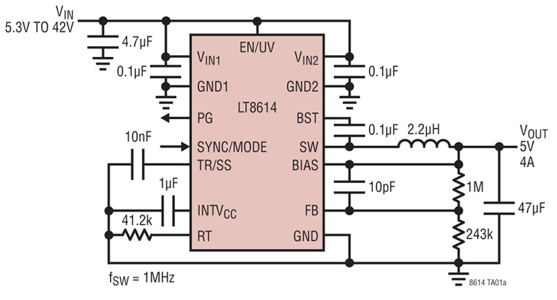
By using a device like Linear’s latest LT8614 Silent Switcher™ regulator, you can have the effect of a shielded box without using a shield and also eliminate the above-mentioned drawbacks (see Figure 1).
Click image to enlarge
Figure 1: The LT8614 Silent Switcher minimizes EMI/EMC emissions while delivering high efficiency at frequencies up to 3MHz.
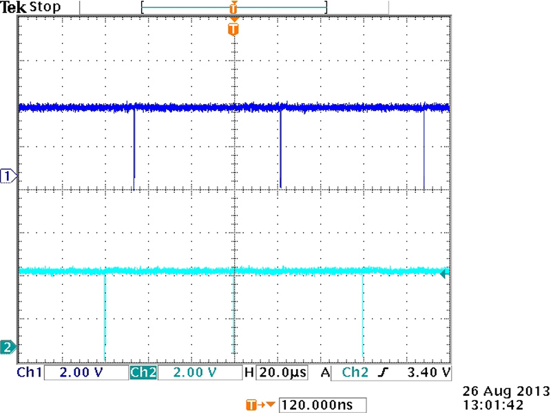
The LT8614 has a low IQ of only 2.5µA operating current. This is the total supply current consumed by the device, in regulation, with no load. The device features the same ultralow dropout of the product family, which is only limited by the internal top switch. Unlike alternative solutions, the LT8614’s RDS(ON) is not limited by maximum duty cycle and minimum off-times. The part skips its switch-off cycles in dropout and performs only the minimum required off cycles to keep the internal top switch boost stage voltage sustained, as shown in Figure 6.
At the same time, the minimum operating input voltage is 2.9V typical (3.4V max.) and the device can supply a 3.3V rail with the part in dropout. The LT8614 is higher efficiency than the LT8610/11 at high currents, since its total switch resistance is lower. It can also be synchronized to an external frequency operating from 200KHz to 3MHz.
The AC switch losses are low so it can be operated at high switching frequencies without much efficiency loss. In EMI-sensitive applications such as automotive environments, a good balance can be attained and the LT8614 can run either below the AM band for even lower EMI, or above the AM band. In a setup with 700KHz operating switching frequency, the standard LT8614 demo board does not exceed the noise floor in a CISPR25 measurement.
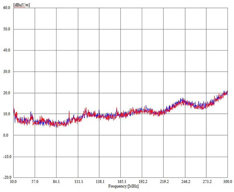
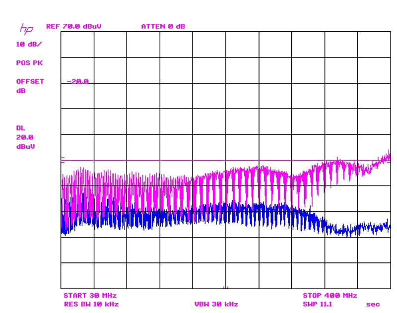
The Figure 2 measurements were taken in an anechoic chamber 12V in 3.3V out at 2A with a fixed switching frequency of 700kHz.
Click image to enlarge
Figure 2: Blue trace is the noise floor; red trace is the LT8614 board at CISPR25 radiated measurement in an anechoic chamber.
To compare the LT8614 Silent Switcher technology against a current state-of-the-art switching regulator, the part was measured against an LT8610. The test was performed in a GTEM cell using the same load, input voltage and the same inductor on the standard demo boards for both parts.
One can see that up to a 20dB improvement is made using the LT8614 Silent Switcher technology compared to the already very good EMI performance of the LT8610, especially in the more difficult to manage higher frequency area. This enables simpler and more compact designs where the LT8614 switching power supply needs less filtering and distance compared to other sensitive systems in the overall design.
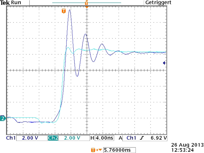
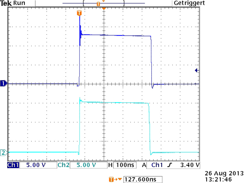
In the time domain, the LT8614 shows very benign behavior on the switch node edges, as shown in Figure 4.
Click image to enlarge
Figure 4: Ch1: LT8610, Ch2: LT8614 switch node rising edge both at 8.4V in, 3.3Vout at 2.2A
Even at 4ns/div the LT8614 Silent Switcher regulator shows very low ringing (see Ch2 in Figure 3). The LT8610 has a good damped ringing (Ch1, Figure 3) but one can see the higher energy stored in the hot loop compared to the LT8614 in Ch2.
Click image to enlarge
Figure 3: Blue trace is the LT8614, purple trace is the LT8610; both 13.5Vin, 3.3V out at 2.2A load.
Figure 5 shows the switch node at 13.2V in. One can see the extremely low deviation from the ideal square wave of the LT8614, shown in Ch2. All time domain measurements in Figures 3 to 5 are done with 500MHz Tektronix P6139A probes with close probe tip shield connection to the PCB GND plane, both on the standard demo boards.
Click image to enlarge
Figure 5: 3 Ch1: LT8610, Ch2: LT8614, both at 13.2V in, 3.3V 2.2A out.
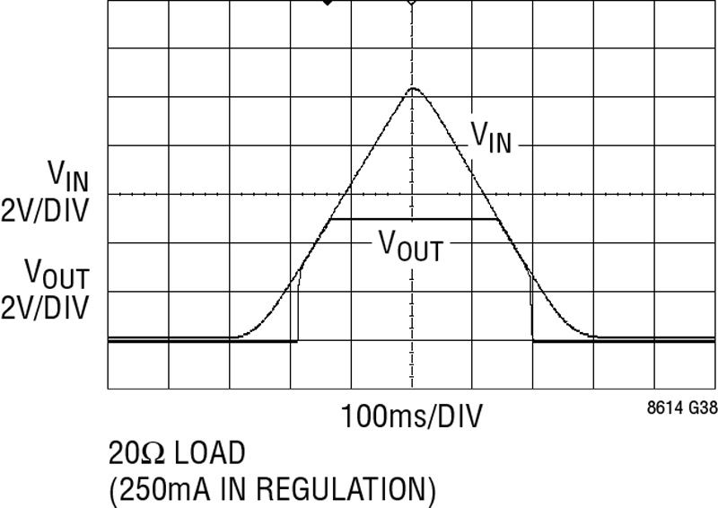
Besides their 42V absolute maximum input voltage rating in automotive environments, the dropout behavior is also very important. Often critical 3.3V logic supplies need to be supported through cold crank situations. The LT8614 Silent Switcher regulator maintains the close to ideal behavior of the LT861x family in this case. Instead of higher undervoltage lockout voltages and maximum duty cycle clamps of alternative parts, the LT8610/11/14 devices operate down to 3.4V and start skipping off cycles as soon as necessary, as shown in Figure 6. This results in the ideal dropout behavior, as shown in Figure 7.
Click image to enlarge
Figure 6: 3 Ch1: LT8610, Ch2: LT8614 switch node dropout behavior
Click image to enlarge
Figure 7: LT8614 dropout behavior
The LT8614’s low minimum on-time of 30ns enables large step-down ratios even at high switching frequencies. As a result, it can supply logic core voltages with a single step-down from inputs up to 42V.
In conclusion, the LT8614 Silent Switcher regulator reduces EMI from current state-of-the-art switching regulators by more than 20dB, while increasing conversion efficiencies with no drawbacks. A 10x improvement of EMI in the frequency range above 30MHz is attained without compromising minimum on- and off-times or efficiency in the same board area. This is accomplished with no special components or shielding, representing a significant breakthrough in switching regulator design. This level of performance in a single IC has not been possible until now. This is just the sort of breakthrough product that allows end-system designers to take their products to the next level.