Occasionally, previously compliant products can fail EMC testing when a MOSFET is replaced with a second-source device with seemingly identical parameters
Figure 1. Nexperia’s 3-phase Motor Control Board and field probes
Equipment constructed using electronic components inevitably generate noise in the form of electromagnetic interference (EMI), with switching components like MOSFETs being the biggest contributors. The level of EMI produced must not exceed values specified for the application, but unfortunately for equipment designers, the level of generated emissions cannot be accurately determined until late in the design cycle when electromagnetic compatibility (EMC) testing is performed on a completed product. Failure to meet specified levels at this stage can require a redesign to include EMI suppression circuity, and this can add extra cost and further delay market introduction.
Even where a product passes EMC testing, a further complication can potentially arise if, due to supply constraints or for other reasons, a second source component is used during manufacturing. This is due to the fact that even though two MOSFETs can have almost identical datasheet specifications, their noise performance can’t be fully evaluated until they are mounted in an application. This means the simple act of swapping a single MOSFET for a seemingly identical alternative from a different manufacturer, a previously compliant product may no longer pass EMC testing.
This article reviews the types of EMI generated by electronic components and typical approaches used by designers to increase the likelihood of their equipment passing EMC testing. It also presents measurements on EMC optimized MOSFETs from Nexperia showing how they reduce the requirement for EMI suppression circuitry while providing designers of new and existing industrial applications with the confidence that their equipment will successfully pass EMC testing.
EMI – Types, Sources and Standards
Modern industrial equipment like motor drives turn on and off large currents in fast switching times.These high frequency voltage and current waveforms have sharp edges that produce large amounts of energy, which causes ringing in their output signals, making them a significantsource of EMI. The two types of EMI emissions areconducted and radiated.
Conducted emissions are carried on wires and traces but because this noise is localized to terminalsor connectorsin a circuit, practicing good board layout and filter design can help with meeting conducted emissions requirements at an early stagein the design process. On the other hand, radiated emissions are more difficult to manage because all current carrying elements on a PCB radiate an electromagnetic field. This means that everytrace on the board acts likean antenna, and copper planes behave likeresonators. All signals apart from an ideal sinewave or DC voltage generate noise right across the signal spectrum. Even with careful design, a designer can only appreciate the full effect ofradiated emissions once EMC testing is performed and unfortunately, radiated emissions testing can only be doneonce the design is finished. CISPR 11 is the international product standard for EMI for industrial, scientific, and medical (ISM) radio frequency (RF) applications. In addition, some industrial end equipment havededicated system-level EMCstandards referenced in CISPR 11. For example, IEC 61800-3 applies toadjustable-speed motor drive systems. Different regions also have their own standards such as the CE mark which appliesin Europe, the Middle East and Africa (EMEA), FCC/UL in the Americas and CCC in China.
Mitigating EMI
EMI cannot be completely eliminated but it can be attenuated to a level at which itdoes not interfere with other equipment. Filteringcan help to mitigate the effects of EMI by reducing the strength of a signal at certainfrequencies. Adding metallic and magnetic shields lowers some of the radiated emissions, while ferrite beads help to reduce conducted emissions on PCB traces. With MOSFETs, the level of EMI produced depends on the features of the device used, including its switching characteristicsand the ability of anoutput network to limit spiking and provide damping for theharmonics it produces. Somedesigners choose to include an external snubber circuitacross each switching devicein order to improve EMC performance, but these are typically device-specific, meaning they arenot normally effective if an alternative (e.g. second-source) MOSFET is used. Sometimes, designers choose to use MOSFETs that havelower values ofRDSon in an attempt to slow down switching and absorb excessive ringing, but these are typically more expensive, therebyincreasing costs and they can unintentionally impact other aspects of product performance.
EMC Optimized MOSFETs
Nexperia’s NextPowerS3 40 V MOSFETs are based on “SchottkyPlus” technology which enables them to deliver high efficiency withlow spiking, features which help to improve EMC performance by up to 6 dB compared to a standard device. This makes them particularly suited for high efficiency applications using fastswitching frequencies where they can reduce costs by mitigating the need to design a snubber circuit or use alternative over-engineered MOSFETs.
Nexperia has focused on balancing the dynamic characteristics of its devices with the increaseddamping required to improve their EMC performance. Apart from being an excellent choice for new designs, these MOSFETs offer exceptional EMC performance even when mounted on boards with sub-optimal board layouts, making them ideal drop-in replacements for existing designs. Figure 1 shows Nexperia’sTrinity 3-phase motor control board which features PSMN3R5-40YSB MOSFETs from the NextPowerS3 portfolio as well as a controller based on non-EMC optimized devices which functioned as a reference control during comparative testing.
Figure 2 graphically illustratesthe results oftests performed using this board which show they deliver an average nose floor improvement of approx. 6-8 dB (in the 125 to 150 MHz frequency range)with improvements of up12 dB at some frequencies, compared to the control devices.
Click image to enlarge
Figure 2. Radiated emissions of NextPowerS3’s 40 V MOSFETs vs. control MOSFETs
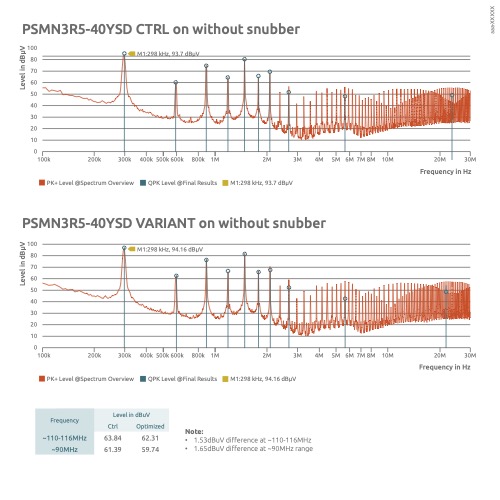
Figure 3 shows the results of comparative testing for conducted emissions using a CISPR25 line impedance stabilization network (LISN) for MOSFETs mounted on the DC1619A evaluation board which features the LT3845AEFE high voltage synchronous current-mode step-down controller with adjustable operating frequency. For test purposes, the snubber circuit was removed from this board, which was also designed to have optimal EMC layout. Notwithstanding these improvements, the overall EMC improvement achieved using the PSMN3R5-40YSB MOSFETs was1.65 dB – a significant improvement over the EMC performance of the control device.
Click image to enlarge
Figure 3. Comparing conducted emissions on a power supply evaluation board
Figure 4 shows that during high current double pulse testing (HCDP) the NextPowerS3 MOSFETs improve damping and spike suppression by up to 17% compared to the control devices, delivering overall EMC performance which meets thetarget value for this application.
Click image to enlarge
Figure 4. Damping factor during HCDP testing showing spike suppression
Conclusion
The level of EMI produced by an electronic product must not exceed values specified for its application, but unfortunately, the level of generated emissions cannot be accurately determined until late in the design cycle when electromagnetic compatibility (EMC) testing is performed. However, a previously compliant product can unexpectedly fail EMC testing by simply replacing a MOSFET with a second-source device with seemingly identical parameters. To reduce the probability of this happening, Nexperia has developed the NextPowerS3 series of EMC optimized MOSFETs which designers can confidently use as either a primary or a secondary source to help their designs pass EMC testing without the requirement for additional snubber circuitry. These are offered in a choice of RDSon and IDmax values and are supplied ina 100% clip-bonded LFPAK56 package. This package offershigh board-level reliability,excellent thermal performance, and is footprint compatible with all major DFN56 packages. Apart from motor drives, other industrial applications for NextPowerS3 MOSFETs includebattery-powered tools, conditioning monitoring, instrumentation, automation and control as well as robots and cobots. These devices can also be used for synchronous rectification in power supplies for telecommunications applications.


