Harvest power & protect battery packs
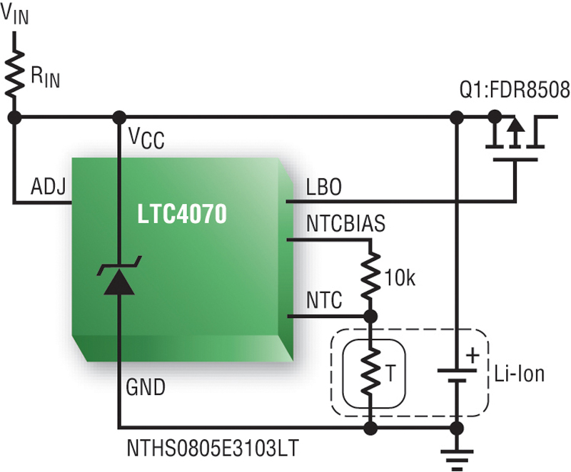
Figure 1: LTC4070 Typical Application Circuit
Energy harvesting ICs can convert an appropriate transducer's output into an electric current for a battery charger device. Recent technology developments have pushed energy harvesting to the point of commercial viability. Many energy harvesting applications inherently have intermittent or low-power sources. And, so many implementations will want to charge a battery for a backup power source. Shunt voltage references are simple to use; they have been around for many years and are in a myriad of products. However, they cannot effectively charge a battery. To configure one to do such a task is extremely cumbersome. Moreover, the ability to accurately and safely charge a Lithium-Ion/Polymer, coin cell or a thin film battery from a low-current source or an intermittent harvested energy source has been difficult to attain safely. Design Challenges for Low Power Consumption Chargers Typical battery charger ICs require a constant DC input voltage and cannot handle bursts of energy. However, intermittent energy harvesting sources such as indoor photovoltaic arrays or piezoelectric transducers provide bursts of power. A unique IC with sub-1uA quiescent operating current is necessary to charge a battery from this type of energy source. Lithium-Ion/Polymer chemistry batteries provide the high performance features necessary for portable electronic devices but must be treated with care. They can become unstable if charged over 100mV beyond their recommended float voltage. Shunt Architecture Basics & Benefits A shunt reference is a current-fed, two terminal device that draws no current until the target voltage is reached and is used like a Zener diode and is often shown on a circuit schematic as a Zener diode. However, most shunt references are actually based on a bandgap reference voltage. This requires only a single external resistor to regulate its output voltage making it extremely easy to use. There is no maximum input voltage limit, and the minimum input voltage is set by the value of the reference voltage because some headroom is required for proper operation. Further, shunt references have good stability over a wide range of currents. Many shunts are also stable with large or small capacitive loads. A Simple Solution Any solution to satisfy the battery charger IC design constraints would have to combine a shunt regulator's characteristics and those of a battery charging IC with the ability to charge from low power continuous or intermittent sources. Such a device would also need to protect and extract the maximum performance from a Lithium-ion/Polymer battery, coin cell, or thin film battery or battery pack. Linear Technology developed the industry's first shunt-architecture battery chargers, the LTC4070 and the LTC4071 to address these applications. With its 450nA operating current, the IC protects batteries and charges them from previously unusable very low current, intermittent or continuous charging sources. The LTC4070's charge current may be boosted from 50mA up to 500mA with the addition of an external PMOS shunt device. An internal thermal battery conditioner reduces the float voltage to protect Li-Ion/Polymer cells at elevated battery temperatures. Multiple-cell battery stacks can be charged and balanced by configuring several LTC4070s in series. Housed in a low profile (0.75mm) 8-lead 2mm x 3mm DFN package, or in an 8-lead MSOP package, the devices are rated for operation from -40°C to 125°C. With pin-selectable settings of 4.0V, 4.1V, and 4.2V, the LTC4070's 1% accurate battery float voltage allows the user to make tradeoffs between battery energy density and lifetime. Independent low battery and high battery supervisory status outputs indicate a discharged or fully charged battery. In conjunction with an external P-FET in series with the load, the low battery status output enables a latch-off function that automatically disconnects the system load from the battery to protect the battery from deep discharge.
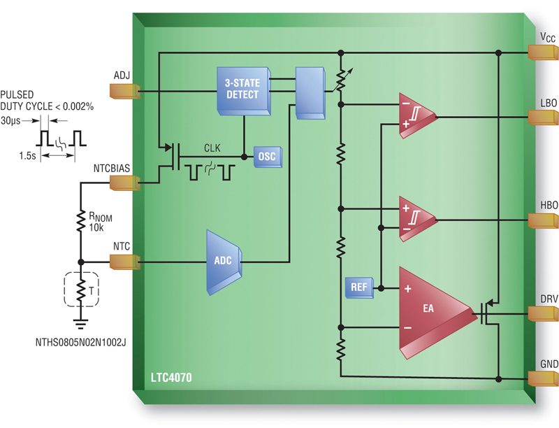
The LTC4070 provides a simple, reliable, and high performance battery protection and charging solution by preventing the battery voltage from exceeding a programmed level. Its shunt architecture requires just one resistor between the input supply and the battery to handle a wide range of battery applications. When the input supply is removed and the battery voltage is below the high battery output threshold, the LTC4070 consumes just 450nA from the battery. While the battery voltage is below the programmed float voltage, the charge rate is determined by the input voltage, the battery voltage, and the input resistor: ICHG = (VIN ? VBAT) / RIN As the battery voltage approaches the float voltage, the LTC4070 shunts current away from the battery thereby reducing the charge current. The LTC4070 can shunt up to 50mA with a float voltage accuracy of ±1% over temperature. The shunt current limits the maximum charge current, but the 50mA internal capability can be increased by adding an external P-channel MOSFET (Figure 1). Internally, the LTC4070 features a P-channel MOSFET being driven by amplifier EA (Figure 2). Zero current will flow in that device until the voltage between VCC and GND reaches VF (i.e. the shunt voltage). VF can be modified by ADJ and NTC, but it is always between 3.8V and 4.2V. If the VCC voltage is below this level, then the current in the PFET is zero. If the voltage across VCC attempts to rise above VF, then current will flow in that device in an attempt to prevent the voltage from rising - this is the shunt current. The operating current is the current required to power all of the rest of the circuitry in the chip. If no external power supply is present, then this is the current that will be drawn from the battery. When the battery voltage is low, more voltage is placed across the input resistor, so the current into the battery (i.e. charge current) is slightly bigger than when the battery is fully charged. When the battery is fully charged, no current goes into the battery, and all of the input current goes into the shunt. Operating current is important because is sets a lower limit on the current capability of "practical" input sources. Obviously, an input source with just 100nA of drive capability would not be able to charge a battery with LTC4070. However, with 1uA of drive capability, there is a small amount of current left to charge. If 10uA of drive capability is available, then more than 90% of that current is available for charging.
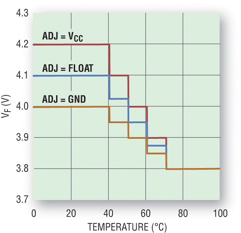
Protecting Batteries The LTC4070 measures battery temperature with a negative temperature coefficient thermistor thermally coupled to the battery. NTC thermistors have temperature characteristics which are specified in resistance-temperature conversion tables. Internal NTC circuitry protects the battery from excessive heat by reducing the float voltage for each 10°C rise in temperature above 40°C (Figure 3). A ratio of resistor values to measure battery temperature. The LTC4070 contains an internal fixed resistor voltage divider from NTCBIAS to GND with four tap points. The voltages at these tap points are periodically compared against the voltage at the NTC pin to measure battery temperature. To conserve power, the battery temperature is measured periodically by biasing the NTCBIAS pin to VCC about once every 1.5 seconds.
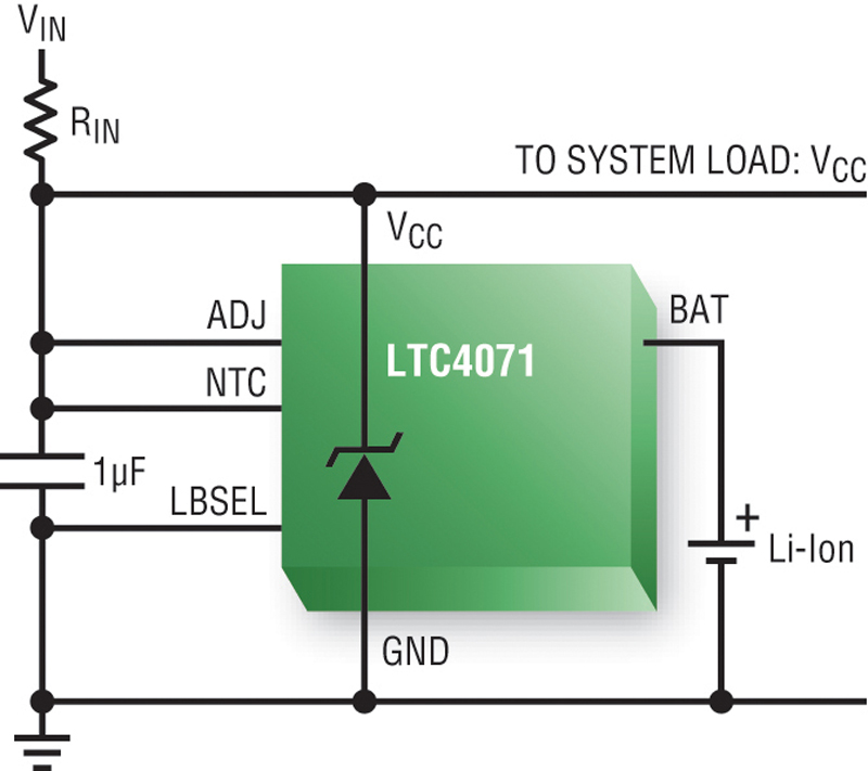
Other Key Features The LTC4070 has a built-in 3-state decoder connected to the ADJ pin to provide three programmable float voltages: 4.0V, 4.1V, or 4.2V. The float voltage is programmed to 4.0V when ADJ is tied to GND, 4.1V when ADJ is floating, and 4.2V when ADJ is tied to VCC. The state of the ADJ pin is sampled about once every 1.5 seconds. When it is being sampled, the LTC4070 applies a relatively low impedance voltage at the ADJ pin. This technique prevents low level board leakage from corrupting the programmed float voltage. Eliminating resistors not only saves solution size but reduces quiescent current as high-valued resistors are not needed. The device also contains status outputs and signaling capability. Battery Pack Protection The LTC4071 is also a shunt battery charger system, and the first with integrated battery pack protection including low battery disconnect but with lower 50mA charge current capability, higher 550nA quiescent current and no LBO. The low battery disconnect is a critical function required to protect low capacity batteries from damage due to self-discharge. LTC4070 can perform a low battery disconnect function with the LBO and an external P-FET, the IC will continue to consume full IQ (about 0.5uA) from the battery. Even this battery drain current can damage a low capacity battery overnight. Conversely, the LTC4071 integrates a complete low battery disconnect which consumes nearly zero current from the battery when disconnected (<1nA at room temperature and <25nA at 125°C). To provide this function in the LTC4071, the LTC4070's LBO and DRV pin have been eliminated (Figure 4). This makes the LTC4071's maximum shunt current fixed at 50mA (LTC4070 is 50mA capable with 500mA possible with an external FET) and increases the IC's quiescent current to 550nA (LTC4070 has 450nA). Conclusion Low-power energy harvesting applications are now primed for conditioning by the right type of DC-DC converter or battery charger. Linear Technology developed the LTC4070 and LTC4071 shunt charger systems for Li-Ion/Polymer cells, coin cells, thin film batteries and battery packs, to provide a simple, effective battery charging and pack protection solution for cutting-edge applications with low-power sources. www.linear.com


