Silicon carbide (SiC) power devices have been used in a wide variety of applications, including server power supplies, energy storage systems, and solar-panel power inverters for a long time.
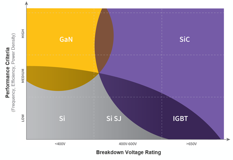
Figure 1: These technologies all have their strengths and application areas in which they fit the best.
The move to electric drive by the automotive industry has recently driven growth in SiC use as well as in design engineer attention toward the benefits of the technology in wider application areas.
Selecting a device technology
No matter what the application, every power supply design starts out by answering the same basic questions: What is voltage in, voltage out, and current out? Next, the designers think about the performance criteria they are trying to enable in their end product. There are a number of technologies at the power supply designer’s disposal today to meet those criteria, including gallium nitride (GaN), SiC, and various silicon (Si)-based technologies like MOSFETs, insulated gate bipolar transistors (IGBTs), and superjunction (SJ) devices (Figure 1).
When the breakdown voltage rating is below 400 V and the design calls for relatively low-frequency operation at less than a kilowatt, silicon is often a good option. When building a compact application, such as a USB charger, that needs a high switching frequency to reduce the size of the magnetics, GaN is an excellent choice. At power levels over a kilowatt and voltage ratings higher than 600 V and up to about 1,700 V at low frequencies, IGBTs can be considered along with SiC. For higher switching frequency or higher power density, however, SiC is the best.
Center of choice
In Figure 1, the moderately high voltages and switching frequencies mark the center of many choices. Yet the high efficiencies offered by SiC make for a compelling option, as weighing BoM cost against operational cost may be a deciding factor.
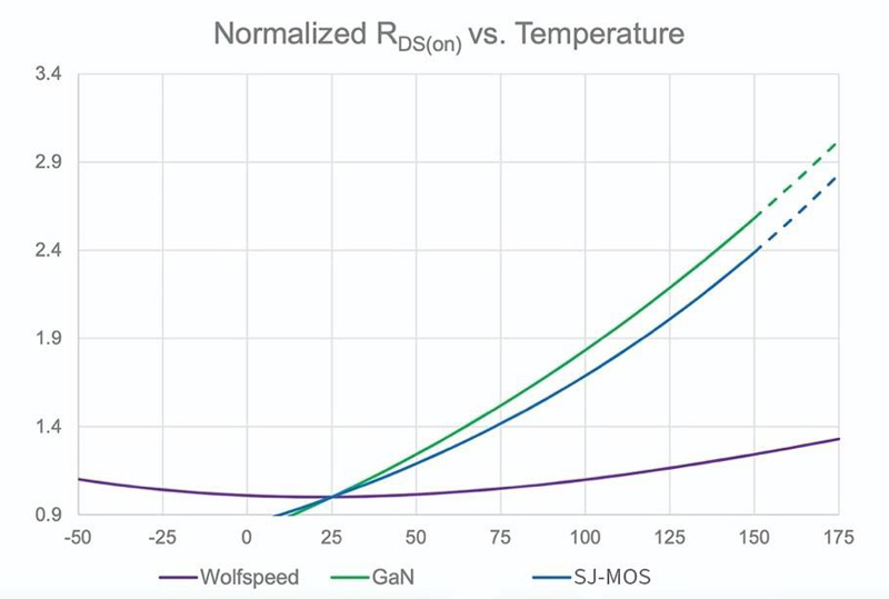
The exceptionally low on-resistance of Wolfspeed’s SiC devices means low conduction losses and higher efficiency. Compared with silicon and GaN in this aspect (Figure 2), SiC outperforms all technologies in all applications. The properties of the material itself enable low change in on-resistance over temperatures, whereas RDS(ON) of GaN and silicon increase by 2.5× or more compared with the rating at room temperature.
Click image to enlarge
Figure 2: Wolfspeed’s SiC devices maintain an unchanging low RDS(ON) over a wide temperature range.
Enabling PFC evolution
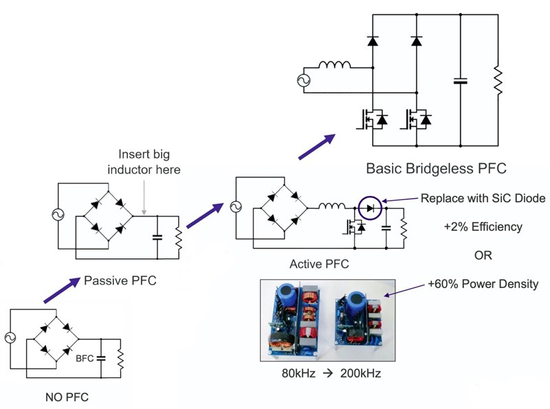
Modern rectifiers for power supplies have evolved from the simple bridge rectifiers that required only a “Big Farad Capacitor” to smooth out the DC output. The addition of a passive power factor correction (PFC) stage typically has an LC filter for the line frequency. This works for relatively low-power applications that do not have stringent efficiency and size requirements (Figure 3).
Click image to enlarge
Figure 3: The evolution of the full-bridge rectifier from simple no-PFC to basic bridgeless PFC
In most switch-mode power supplies today, the boost converter is used after the diode bridge as active PFC that switches several orders of magnitude higher than the line frequency so that smaller inductors and capacitors can be used. Depending on the application, replacing a silicon-based diode with a SiC diode in the active PFC stage can increase efficiency by two to three percentage points.
On the other hand, increasing the switching frequency from 80 kHz to 200 kHz can reduce the form factor or increase power density by as much as 60%. In general, increasing switching frequency helps reduce the size of the inductor and therefore the copper losses in the inductor as well.
When going from 200 kHz to 400 kHz, however, a leveling-out of the copper losses is seen while the inductor core losses continue to increase. The result is diminishing returns, where a 10% to 15% reduction in size is accompanied by a 10% to 15% increase in power loss. This may be an acceptable tradeoff for applications in which size reduction is paramount.
To take the efficiency levels into the higher 90s, the circuit must be redrawn in a way that removes the diode bridge. One way to do this in the boost implementation is to move the inductor to the AC input and swap out the two bottom diodes in the bridge with two MOSFETs. The switch on the left boosts the voltage on the positive half cycle, while the one on the right boosts on the negative half cycle.
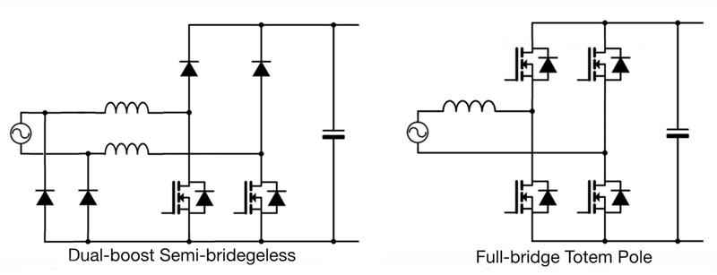
The challenge with the basic bridgeless circuit is that the high-frequency switch node is connected directly to the AC input and the DC ground is floating relative to the AC input. This can cause any parasitic capacitance to go straight into common-mode EMI. A common way around this is to use a dual-boost or semi-bridgeless implementation (Figure 4, left).
Click image to enlarge
Figure 4: Comparing the dual-boost semi-bridgeless solution (left) with the full-bridge evolution to totem pole topology (right) made possible by SiC
In this topology, the two diodes on the bottom left eliminate the floating ground problem and splitting up the inductor eliminates the direct connection of the switch node to the AC source in order to take care of the common-mode EMI problem. While silicon MOSFETs can be used, they result in a maximum efficiency of 95% to 96%, a larger footprint, two inductors, and a potentially higher total BoM cost.
Totem pole topology
An alternative to the dual-boost semi-bridgeless configuration is the totem pole topology that gets its name from the manner in which transistors are stacked on top of each other (Figure 4, right). The totem pole can be built as a full-bridge version, as shown, or as a bridgeless version with the MOSFETs in the low-frequency leg on the right replaced by diodes.
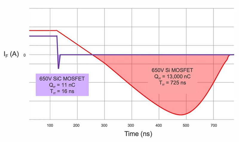
The big challenge with totem pole topologies is the reverse-recovery charge of the MOSFET body diode if the converter works in continuous conduction mode (CCM) condition. During the transition from low-side to high-side switches, both FETs cannot be on at the same time, and the body diodes have to conduct during that dead time. The reverse-recovery characteristics of silicon eliminate the efficiency (Figure 5).
Click image to enlarge
Figure 5: SiC vs. Si body-diode reverse-recovery comparison
In all hard-switching power supply designs, when the body diode has to conduct, there are reverse-recovery losses. With SiC, which has no minority carriers, there is nearly zero reverse-recovery current.
The silicon MOSFET, on the other hand, suffers from several orders of magnitude higher losses. This is what makes silicon unusable in the totem pole.
Full-bridge or hybrid totem pole?
The fully synchronous version of the totem pole is the most efficient implementation. While it can use silicon MOSFETs in the low-frequency leg, only the all-four SiC MOSFET implementation enables bidirectionality — for instance, in applications that connect to a smart grid, with some tradeoff in complexity and BoM cost.
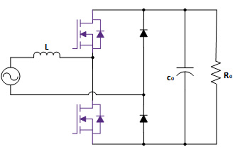
Most cost-sensitive applications, including server power supplies, use a bridgeless or “hybrid” totem pole topology using inexpensive PIN diodes on the low-frequency leg (Figure 6). It has the advantage of using the fewest number of components and, with the introduction of Wolfspeed’s C3M SiC MOSFETs in the 650-V class, it is a cost-effective implementation with less than 0.5% decrease in light load efficiency compared to a full bridge.
Click image to enlarge
Figure 6: “Hybrid” Totem Pole Topology using SiC MOSFETs and diodes
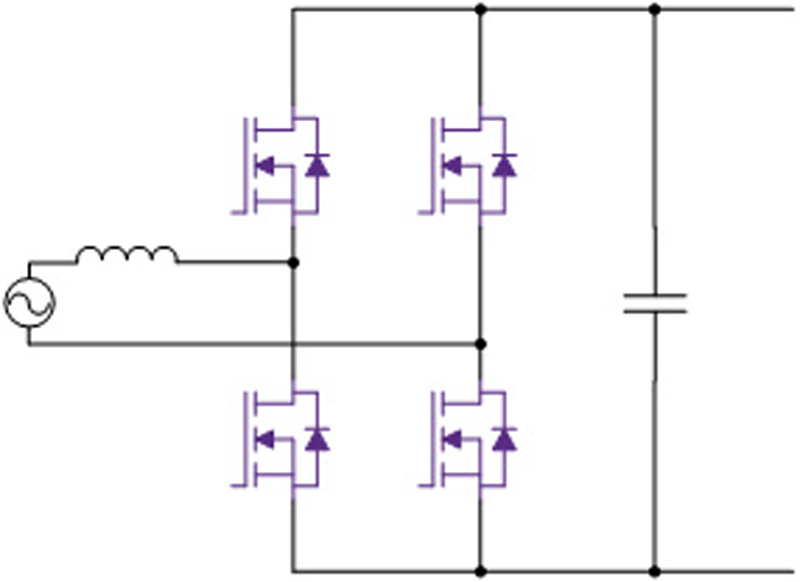
However, as shown in Figure 7, to achieve the full potential of totem-pole PFC topology and higher than 99% peak efficiency, the full-bridge totem-pole PFC that utilizes all four SiC MOSFETs thus eliminates diode voltage drop enables the highest efficiency and power density.
Click image to enlarge
Figure 7: Full-Bridge Totem-pole PFC with all SiC MOSFETs
This has already been proved by Wolfspeed’s CRD-03600AD065E-L 3.6 kW reference design that is available for download as a package comprising BoM, schematic, board layout, presentation, and application note. It uses Wolfspeed’s latest 650 V 45 mΩ MOSFETs in a compact, low profile TOLL package to achieve >99% efficiency as well as 92W/in3 power density.
SiC-based totem pole designs like this provide the highest possible efficiency for AC-DC conversion, enabling engineers to design systems that meet or exceed the most stringent efficiency requirements such as the 80+ Titanium standard.
To simulate your own design, use the online SpeedFit™ Design Simulator or SpeedVal Kit™ Modular Evaluation Platform, which provides a flexible set of building blocks for in-circuit evaluation of system performance. Have questions? Connect with Wolfspeed Silicon Carbide power experts at our Power Applications Forum, or brows our Documents, Tools & Support section of our website.

.jpg)