Bizen technology has been verified by physical wafer results to deliver the same voltage levels, switching speeds and power handling of wide bandgap devices.
The claim is made by developer Search For The Next (SFN).
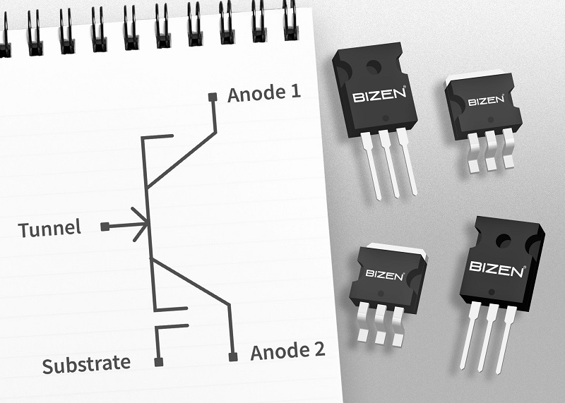
The first devices to use Bizen are members of the QJT (Quantum Junction Transistor) family which will include three parts rated at 1200V/75A, 900V/75A and 650V/32A, available in the industry-standard TO247 or TO263 power MOSFET packages. Of extreme significance is that these devices can be made using standard silicon substrates on conventional, larger-geometry silicon processing lines.
Explains David Summerland, CEO and founder of Nottingham-based Search For The Next (SFN) which invented the Bizen technology: “To get this level of performance from traditional silicon-based MOSFETs, the device size must be much bigger. 1200V/75A in a TO247 housing can be achieved using wide bandgap materials like silicon carbide, but this approach has other well-known issues. SiC, for example, takes much longer to process and has a significant manufacturing carbon footprint. Also, regardless of the roadmaps, SiC does not scale like silicon, and the economic argument that SiC can match silicon does not take into account the advances made possible by Bizen. By contrast, the data we have obtained from physical wafer tests proves that by using Bizen on silicon substrates, our QJTs deliver the same performance as SiC or GaN. Yet the production equipment required to make a QJT is exactly the same as for a standard silicon MOSFET, and the Bizen process adds no extra manufacturing complexity.”
Bizen applies quantum mechanics to a traditional bipolar wafer process. The result is a very rugged and reliable device with the heritage and pedigree of traditional bipolar silicon technology. Bizen also reduces leadtimes from 15 weeks – typical for integrating MOS to create large scale integration CMOS – to less than two weeks, and halves the number of process layers; the new QJTs use these same eight layers and wafer process.
Wafer tests also show that the Bizen process exhibits an effective current gain of over 1 million. This will enable direct connection between the 1200V/75A QJT power transistor and a low voltage, low current CPU output port such as a PWM. Concludes Summerland: “The QJT is the first power device on the Bizen family roadmap. This will shortly lead to the PJT (Processor Junction Transistor), an integrated Bizen device with its own processor which can also be produced on a manufacturing cycle time of eight days, heralding a new era of intelligent power devices.”
SFN has also released other comparative performance metrics for a 1200V/100A part – also in TO247 – which is on its short-term roadmap. The losses at rated current will be one quarter (<300mV) of those exhibited by the SiC device, and its input capacitance will also be four to five times less (< 1pF).
https://www.wafertrain.com/blog