The Olympic generation of automotive video interfaces
According to IMS Research the number of video capable automotive head units will grow from 8.5 Mu in 2006 to 26.6 Mu in 2015. In order to present the information to the driver with less distraction from car traffic, the displays will need to be installed in places which are remote from the actual head unit, e.g. in the top area of the middle console, the instrument cluster or as head up displays, projecting to the back of the windscreen. The video interfaces, tying graphics sources and panels together, are more and more converting from analog video technology to the higher quality RGB (Red Green Blue) digital video format which is the standard interface used within LCD displays. While for the front display applications cable lengths typically stay in the range of 1-3 meters, the Rear Seat Entertainment (RSE) units on the other hand can require cable reach of 8 meters and beyond. Such connections supporting data rates in the Gigabit/sec region, far beyond the baud rates of conventional automotive board networks, can nicely be addressed with point-to-point Serializer/Deserializer (SerDes) solutions. Such chipsets greatly reduce the number of transfer wires and connector pins in comparison to transporting a wide, parallel video bus thus offering tremendous system-level advantages. The DS90UR905/6 and DS90UR907/8 SerDes chipsets have been developed by National Semiconductor to address the especially harsh requirements for automotive display interfaces in terms of high data throughput, ultrathin cabling, advanced signal conditioning, testability and ultra-low EMI (Electro Magnetic Interference). They represent the industry's first embedded clock SerDes solutions to span resolutions from Quarter Wide VGA (400 x 240) and up to XGA (1024 x 768) at 24-bit color depth. This wide range of pixel clock frequencies allows the car manufacturers to employ just one digital video display interface solution throughout their portfolio of car models from small instrument cluster panels over dual view, center stack LCDs to larger format RSE displays.
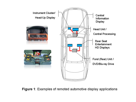
The targeted application for the SerDes components is a Flat Panel Display Link interface connecting a graphic host to a display over a long serial cable. Typical examples range from Central Information Displays (CID) to instrument cluster panels to entertainment LCDs in the headrest or flip-down modules from the roof for rear seat passengers as shown in Figure 1.
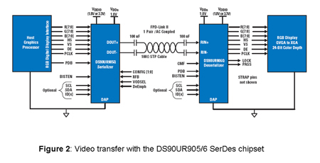
These new chipsets are part of the "FPD-Link II" product family of National Semiconductor and translate 27 bits of digital RGB color and timing control signals from a video source into one single, serial data stream with embedded clock information over a twisted pair of wires. This video transfer concept is depicted in Figure 2 on a system level.
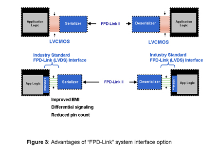
The chipsets can support either 18-bpp (bits per pixel) or 24-bpp color depth applications. The pixel clock range has been designed to be extremely wide from 5MHz up to 65MHz frequency. This translates in serial line rates from 140Mbps (bits per second) to 1.82Gbps, covering all mainstream resolutions of automotive displays. The SerDes chipsets require NO external reference clock (quartz or oscillator) to "pre-synchronize" the receiver's PLL within a certain frequency band around the transmitter's parallel clock. The DS90UR907/8 chipset has the same features as the DS90UR905/6 chipset with the difference that the inputs and outputs are no longer parallel busses with LVCMOS signaling, but still comply with the open-industry "FPD-Link" standard. Many state-of-the-art graphic controllers, display timing controllers, ASICs and FPGAs support this "first level of serialization" which employs either 3 data lanes for 18bpp or 4 data lanes for 24bpp, each with a parallel clock channel. The electrical signaling is according to the open ANSI/TIA/EIA-644A standard, also known as "LVDS" (Low Voltage Differential Signaling). The advantages of using this interface option instead of the conventional LVCMOS are lower EMI levels through differential signaling and reduction of component pin count, as illustrated in Figure 3.
Both display and camera applications can greatly benefit from having the power transferred from their respective link partners over the video data cable. In the case of a navigation panel the power could be sourced from the head unit and in the case of a camera imager the power could come from its respective electronic control unit. The main advantage of such concepts is the significant reduction of the overall cable harness and board connectors. This can lower cabling cost and weight, while enabling the smaller footprint designs that can be essential for tiny imager modules used, for instance, in outside mirror locations.
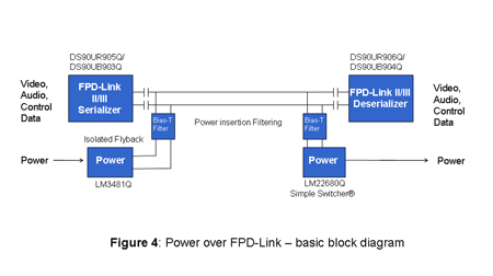
Figure 4 shows a block diagram on how power can even be inserted and extracted on the very same pair of wires, that National Semiconductor FPD-Link II and FPD-Link III chipsets are using for video, audio and data transfer. Hence this approach is called "Power over FPD-Link". This topology is needed for a solid powered data line. A Bias-T filtering is recommended for a close to noiseless power insertion, which isolates the high-speed data from the power line. A ground isolation topology (with isolated flyback) avoids the return current through the boost converter path. The overall performance depends of course strongly on the system ground and shielding concepts. In practical setups power ratings of over 25 Watts could be achieved at the remote link partner, when working with insert voltages of 12-14 Volts (from car battery). This easily accommodates the power consumption of driver assistance camera modules (1-3 Watts) and most standard infotainment displays (15-20 Watts).
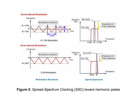
The deserializer is enhanced with an integrated, configurable Spread-Spectrum Clock (SSC) generator. At the receiver output bus this leads to a slight variation of the output clock frequency and data spectrum over time at very low modulation rate of a couple ten kiloHertz. As described in Figure 5, the frequency variation can happen around the nominal pixel clock center frequency ("center spread modulation") or towards lower frequencies ("down spread modulation"). The spreading of the spectrum can be as high as plus or minus 2%. Instead of switching all outputs at the same point in time and at a constant frequency while exhibiting a narrow band of radiation noise, the Spread-Spectrum Clocking is distributing the peak energy over a wider spectral range, thus reducing the EMI noise level significantly. With all output data synchronized to the output clock, both data and clock are effectively spread. Particularly with the Low Voltage (LV) CMOS interface option at the DS90UR906 receiver output, this feature can drastically reduce electromagnetic radiation. Further enhancements include the integrated termination resistors, which reduce the complexity of the board design and lead to lower cost and less board space. The chipset supports a very wide temperature range of -40°C to +105°C. This opens application areas in a variety of automotive electronics systems where displays need to be exposed to very high or very low temperature environments. The chipsets are offered in small footprint, Leadless Leadframe Package (LLP) options at a mere 1mm thickness, which are of course lead free and RoHS compliant. This industry standard packaging type exhibits outstanding electrical and thermal characteristics and is well suited for standard manufacturing handling and inspection. Not at last the chipsets are fully automotive qualified according to AEC-Q100 Grade 2 standard.
The new DS90UR905/6 and DS90UR907/8 FPD-Link II chipsets deliver many strong system benefits and enhancements. The parallel video bus is serialized into a single pair with an embedded clock. This lowers system cost, eliminates clock/data skew issues, reduces noise, and extends the link to long cable distances. The chipsets support all common automotive LCD resolutions from QWVGA to XGA at 24-bit color depth. Special attention has been paid to EMI mitigation features in order to facilitate system design, qualification and approval. Consequently this minimizes expensive shielding requirements, while not sacrificing robustness. The FPD-Link II chipset family represents an automotive optimized, true plug ‘n' play solution due to its no compromise combination of low wire count, high bandwidth, low power, low EMI, ruggedness and autonomous link synchronization. Not at last it has been demonstrated that power transfer concepts can use the same pair of wires without disturbing the video link, enabling lighter, cheaper cable assemblies and less, smaller form factor board connectors to be used. www.national.com
DS90UR905/6 Product folder: http://www.national.com/mpf/DS/DS90UR905Q.html DS90UR907/8 Product folder: http://www.national.com/pf/DS/DS90UR907Q.html LVDS Owner's Manual: http://www.national.com/analog/interface/lvds_owners_manual