The switch node of a switching regulator or power converter circuit is a critical conduction path that requires special attention when designing the PCB layout
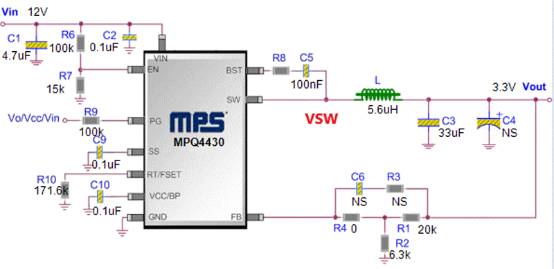
Figure 1: MPQ4430 Buck Converter Example
The circuit node is where one or more power semiconductor switches (such as a MOSFET or diode) connect to a magnetic energy-storing device (such as an inductor or transformer winding). The switching signals of this circuit node contain fast-switching dV/dt voltages and dI/dt currents that can easily couple onto surrounding circuits and create noise problems, which can prevent the PCB and system from passing stringent electromagnetic compatibility (EMC) requirements.
This article will provide a basic review to learn about switch node waveforms, properly size a switching (SW) trace for PCB routing, and understand the near-field coupling effects of E-fields and H-fields from the switch node.
Switch Node Waveforms
Understanding the current and voltage waveforms on the switch node is the first step in preparing for the PCB design of this critical trace. In particular, waveforms for switching voltages, time-varying current, and switching frequency should be reviewed and understood before attempting the layout.
Consider a step-down (buck) converter like the MPQ4430 (see Figure 1). This device from Monolithic Power Systems (MPS) has integrated high-side and low-side FETs, and is capable of providing up to 3.5A of load current.
In this example, which uses MPS’s DC/DC Designer Online tool, the MPQ4430 regulator is designed to step down from 12V to 3.3V while providing a maximum load of 3A. The switch node in Figure 1 is labeled VSW in red. Note that “VSW” and “the SW node” are used interchangeably in this article, and both describe the switch node.
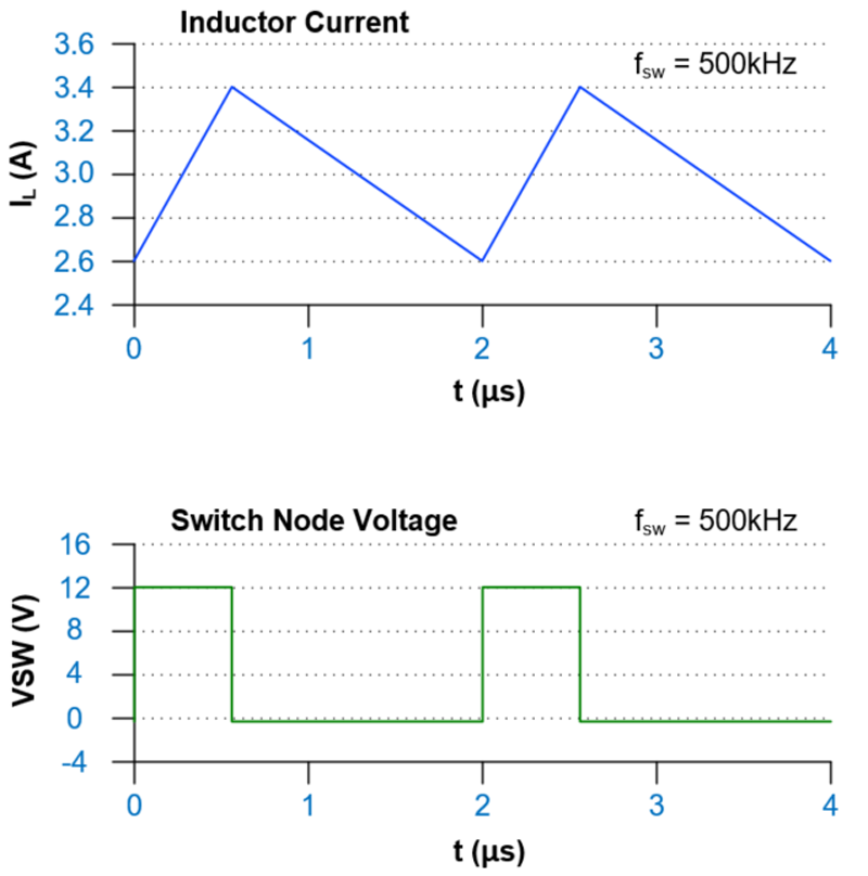
The waveforms in Figure 2 show the switching voltage and inductor current measured on the switch node. The voltage waveform switches between 12V and just below 0V at a rate of 500kHz, with very fast rise/fall times in the low nanosecond range. This large dV/dt creates a strong electric field (E-field), which has a significant noise spectrum up into the tens and hundreds of MHz.
Click image to enlarge
Figure 2: Switch Node Waveforms for the Buck Converter
Since the buck converter operates in continuous conduction mode, the inductor current is always positive and never reaches 0A. The current ramps up to about 3.4A during the on cycle of the buck converter, and down to about 2.6A during the off cycle. The current has an average value of 3A to supply the load. The inductor opposes fast changes in current, so the current waveform does not have sharp transition edges like the switching voltage. Even though dI/dt is not very large, there is still a ripple current with a strong time-varying magnetic field (H-field) at the 500kHz switching frequency. This H-field can be a potential issue for nearby circuits that are sensitive to this frequency range.
Minimizing SW Node Trace Length
The switch node trace is meant to carry a relatively large time-varying current for a short distance. The inductor should be placed very close to the SW pin on the regulator. A short connection minimizes coupling of high-frequency E-fields from the high dV/dt waveform, as well as the lower-frequency H-field from the inductor ripple current.
Figure 3 shows how to route the switch node by placing the inductor close to the regulator. When designing the PCB layout, it is important to leave a small area between the converter and inductor for other components that must be connected to the SW node (e.g. a small bootstrap capacitor). These components should be placed such that they minimize the length of the SW trace.

Click image to enlarge
Figure 3: Switch Node Layout for 3A Buck Converter on 4-Layer PCB
Figure 3 shows that the bootstrap capacitor should be placed so that its longest dimension is perpendicular to the SW trace. This reduces extra length between the SW pin and inductor. Even though the capacitor pushes the inductor out slightly, it is still possible to achieve a very short distance of approximately 3mm to 4mm. The VSW trace length varies depending on the application and size of the components, and in some cases may be longer than what is shown in this example.
Sizing the SW Node for Current
The connection from the regulator’s SW pin to the inductor’s input side is normally a wider trace than other signal traces on the PCB. It is recommended to create a wide trace or copper pour that has the following characteristics:
1. Uses sufficient copper thickness and a sufficient trace width to handle the current requirements.
2. Keeps the length as short as possible to minimize near-field coupling to other circuits.
The width of the SW node trace is critical for handling the required current supplied to the inductor. For our buck converter example, the average current delivered to the inductor is the same as the average output current (3A). The design engineer should specify the maximum current condition, which can then be used to estimate the width of the SW node.
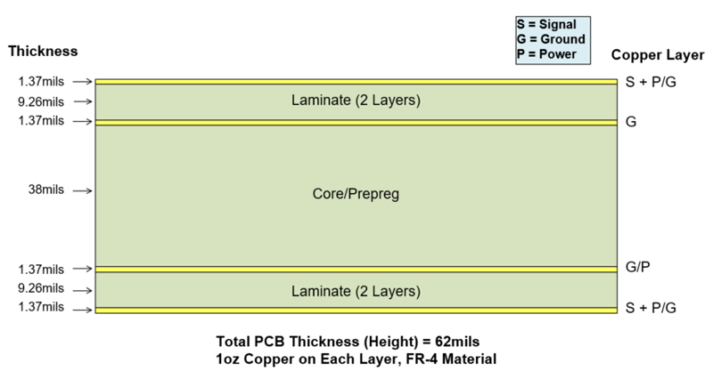
For our design example, assume a 4-layer PCB uses 1oz copper on the top, bottom, and inner layers (see Figure 4). The switching regulator circuit is placed and routed on the top layer, and the ground (GND) return plane is 9.26mils (about 10mils) below the top layer. We can use one of many available calculator tools (found in PCB CAD software, or on PCB manufacturers’ websites) to properly size the conductor for the current.
Click image to enlarge
Figure 4: 4-Layer Stackup Used for the 3A Buck Converter
If we design for a 3A maximum load and try to limit the temperature rise of the PCB to 10°C, we calculate that a 50mil width can accommodate close to 3.5A for this 4-layer stackup. A 50mil switch node width is a good target for this design, since it provides some margin above the 3A maximum load. Different tradeoffs can be made based on the allowable temperature rise of the PCB. While it is common to see the trace sized to be as wide as the inductor pad, we can see from this case that a narrower trace is fully capable of meeting current and thermal requirements.
Note that the calculator used to size the conductor for the current should follow the latest IPC2152 standards, as opposed to the older IPC2221. This is especially crucial for multi-layer PCBs. IPC2152-based calculators are more accurate, and account for factors such as PCB thickness,PCB thermal conductivity, trace thickness, and distance from the trace to copper planes.
SW Node E-Field and H-Field
A switch node trace consists of a PCB trace above a reference plane, and can be viewed as a significantly shortened version of a microstrip line, particularly at high frequencies. A microstrip line with controllable impedance is used in high-speed transmission line applications for digital, high-speed analog, and radio frequency (RF) signals. Even though the applications for a switch node and microstrip transmission line are different for the intended signals they conduct, their geometries exhibit similar properties for time-varying electric and magnetic fields.
Figure 5 shows E-fields and H-fields from the switching voltages and time-varying currents on the SW trace. The SW trace width (w) is placed at a height (h) above a return plane. E-field lines of flux extend from the top, bottom, and sides of the SW trace. The strongest E-field concentration, especially at high frequencies, occurs along the bottom and edges of the trace, which are in close proximity to the return plane.

Click image to enlarge
Figure 5: Switch Node E-Field & H-Field
At high frequencies, currents will be present where the E-field lines terminate on the return plane. To better contain the E-field and reduce parasitic near-field coupling, it’s best to minimize the distance (h) between the return plane and the SW trace, and to increase distance between the SW trace and surrounding circuits as much as possible.
The ripple current in the SW trace creates a time-varying H-field that surrounds the trace. The magnetic flux from the H-field can inductively couple onto nearby sensitive circuits through mutual inductance of the circuits. Similar to E-fields, the best way to contain the H-field is to have the return plane as close as possible to the SW trace by minimizing h, while simultaneously increasing distance between the SW trace and surrounding circuits. A dedicated GND return plane placed close to the SW node is a great approach to provide very good field containment.
Conclusion
For any switching regulator or power converter circuit, the layout of the SW node requires serious consideration. It is important to understand SW node waveforms, determine a reasonable SW trace size, and utilize strategies to minimize near-field coupling.
The first step is to fully understand the switching voltage waveforms, current waveforms, and switching frequency. Next, determine the SW trace width based on the maximum current requirements, then minimize the SW trace length. Finally, allow sufficient spacing between the SW node, surrounding ICs, and circuits to minimize near-field coupling. When using a multi-layer PCB stackup, always place a GND return plane directly under the SW trace, and ensure the trace is as close to the GND plane as possible. This further minimizes near-field coupling of the E- and H-fields from the SW node.
Following these steps while designing the PCB layout will help achieve a better EMC design!


