The Future of MicroLED Displays Using Next-Generation Technologies

MicroLEDs offer an emissive display technology that delivers high contrast, high speed and a wide viewing angle current without high power consumption
MicroLEDs (micro-light-emitting diodes) are an emerging display technology that, as the name implies, use very small LEDs for pixels. Much the same as any other current display technology, it combines red, green and blue sub-pixels to reproduce a colour. Although there are currently no microLED displays in mass production today, there is a massive opportunity for the technology to penetrate major display markets and replace incumbent LCD and OLED (organic light-emitting diode) technologies in a wide range of applications, from HDTVs to smartphones and wearables such as smart watches, and head-up displays (HUDs) and virtual reality (VR) and augmented reality (AR) headsets. According to research consultancy Yole Développement, the market for microLED displays could reach up to 330 million units by 2025. However, many development challenges remain before microLEDs can fully realise their potential.
Display Technologies
Like OLEDs, microLEDs offer an emissive display technology that delivers high contrast, high speed and a wide viewing angle current. However, OLED technology is power hungry and does not offer high levels of brightness – for example, users will often find it difficult to read the screen of a smartphone or tablet in high ambient light. Whereas MicroLEDs offer the potential for significantly higher brightness, as well as enhanced robustness and longer lifetime. In addition, a major advantage is greater efficiency, which can mean significantly reduced power consumption, making the technology ideal for battery powered products.
MicroLEDs are also ideal for small form factor products such as head-mounted displays, making VR and AR a major application opportunity. However, in these types of applications there are difficulties concerning waveguide interfacing, as LEDs are typically coupled with a waveguide to deliver the image, in contrast to a smartwatch for example, which has a directly viewable display. Coupling a waveguide is a very lossy process: only 7% of the light entering an HUD is usable by a viewer, with 93% being lost. Although this is perhaps acceptable for relatively simple applications, such as displaying vehicle speed or satnav information, it is unsuited to more complex images.
Importantly, microLEDs start off as a significantly brighter source, offering brightness three or four orders of magnitude higher than OLEDs, which are capable of delivering around 1000 Nits (cd/m2), whereas microLEDs offer hundreds of thousands of Nits for the equivalent power consumption. This is a major advantage in devices from HUDs to VR and AR products, where waveguides are commonly used to place images in a headset or in a pair of glasses right in front of the eye. The vision for microLEDs could mean the transformation from a typical bulky and power-hungry VR headset to something more akin to a pair of glasses. Alternatively, it could mean charging every month rather than every two days for a product in which the display is largely responsible for the majority of the power consumption.

Click image to enlarge
Figure 2. AR Glasses
Manufacturing
A major challenge existing today for the manufacture of microLED displays is placement of gallium nitride (GaN) LEDs onto a substrate. One notable approach in the industry is the development of GaN-on-sapphire technology, but this technology is not suited to a monolithic approach and is currently achieved using pick-and-place equipment. This involves the individual placement of every LED on a pitch of less than 50μm, which requires new and expensive equipment that is subject to productivity issues. However, with increasing pixel density for displays, the LED pitch becomes ever smaller and pick-and-place becomes less feasible both commercially and technically. There is much development in the industry in pick-and-place manufacturing technology, with the emphasis on massively parallel processing equipment that can simultaneously pick up hundreds or even thousands of LEDs from the donor wafer and then attach them to a backplane, but clearly this means significant capital expenditure. Another issue with increasing pixel density is that discrete LEDs have a finite size, bringing issues of physical stability as well as alignment. The human eye is most unforgiving – it is very good at picking up distorted images or misalignment from pixel to pixel. Certainly, massively parallel pick-and-place production can help, but it must be recognised that the spacing between each individual LED will still be limited by its size.
GaN-on-sapphire technology typically targets high-volume applications such as smartphones or smart watches that might typically offer 400dpi displays, based on an 80-micron pixel pitch. But moving to VR, AR or merged-reality applications means the pixel pitch needs to be reduced to 40 or 20 microns, or even as low as 10 to 15 microns. It is beyond the ability of pick-and-place machinery to place pixels with any kind of alignment accuracy.
In order to address cost and yield considerations, there will also be a requirement to build micro LED arrays on larger substrates. GaN-on-Sapphire substrates exist up to 6”, but the costs to increase sapphire substrates to 200mm will result in very expensive substrates. In addition to the availability of large GaN-on-sapphire wafers, another point is that it is very difficult to scale up the size of an LED array using GaN-on-sapphire. A significant advantage of an alternative technology – GaN-on-Silicon (Si) – is the ability to make much larger LED emitters. One major reason is that GaN-on-Si is an inherently surface-emitting technology, whereas GaN-on-sapphire is an inherently volume-emitting technology – emitting from all four sides of the device as well as the surface. In the development of advanced display technologies, it will be necessary to resolve individual pixels and colours, and a volume-emitting LED delivers a significant amount of cross-talk from individual pixels, resulting in a loss of contrast for an end display.
Monolithic Approach
All this leads to the construction of a single hybridised monolithic array, which is to say, building GaN microLEDs on top of, and interconnected with, a CMOS silicon thin-film-transistor backplane with no requirement for pick-and-place. Very importantly, this approach supports the integration of a standard CMOS circuitry array that delivers charge to the LEDs, providing the necessary addressing and driving of microLED displays. In addition, this approach can enable the close integration of high-performance GPUs, all of which can be carried out using standard CMOS manufacturing methods. A major point is manufacturing scalability – monolithic GaN-on-Si is very easily scalable to 200mm wafers and beyond, which will be critical for cost and yield.
Certainly, monolithic microLED manufacturing is a nascent technology and many challenges remain. Not least of these is connected with colourisation issues; further research is required into the properties of phosphor, as well as other potential materials, for the conversion of blue light into green and red, especially when making a 5- or 10-micron pixel.
Overall, moving to a monolithic process will enable smaller and higher-resolution displays for a range of applications, and GaN-on-silicon is the only technology that can deliver the required levels of scalability and performance. It offers higher luminosity than OLED and also better thermal conductivity than sapphire and is becoming widely acknowledged as the best bet to deliver the next generation of high-resolution and high-luminance displays.
Developing the Right Technologies
Plessey Semiconductors is a leading developer of award-winning optoelectronic technology solutions, with extensive expertise in LED technologies.For the past five years, the company has been developing highly efficient and robust products that target the high-power LED lighting market, based on technology gained in 2012 from the company’s acquisition of CamGaN, a spin-out from Cambridge University. Prior to this, Plessey was a leading European foundry for CMOS image sensor production.
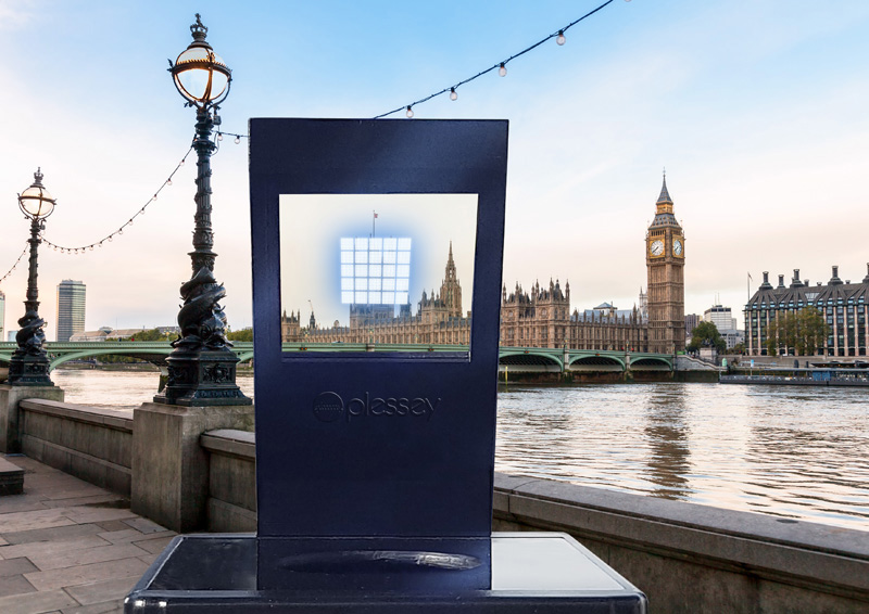
Click image to enlarge
Figure 3. Product Demonstrator
Experience gained in these markets provides the company with a significant head-start in knowing how to design the backplane to be used with a microLED display, especially in terms of understanding yield issues. In addition, the underlying principles of LED displays and image sensor technologies have much in common: the light-sensing component of the CMOS sensor is essentially replaced with the light-emitting component of the microLED. The principles in driving and addressing LEDs are similar and the clocking of data is also analogue – in for LEDs and out for image sensors. In addition, many functional blocks are similar, if not entirely the same. This experience, in conjunction the development of significant range of technological IP,is enabling the move to the next step in the company’s evolution: Plessey is to license out its production-ready GaN-on-Si technology platform to potential microLED display makers.
The company has made several important steps in the development of microLED technology, which is already offering LED performance that is equivalent to incumbent technologies in general lighting applications. The company has already demonstrated its capabilities with the development of 100- and 20-micron pitch LED arrays for a print-head project with LumeJet, based on blue microLEDs and offering a density of 400 pixels per inch (ppi). A 100-micron microLED demonstrator already exists, and Plessey will be offering a 20-micron version in 2018. Technology demonstrators at 100 microns are now also in development from Plessey for red and green microLEDs. The company is already deep into a development programme to address the challenges for sub-10-micron pixel applications.
While many challenges still exist, the monolithic GaN-on-Si approach for microLED technology is not subject to the technical and commercial productivity issues associated with pick-and-place equipment. Overall, it can deliver the high-volume and cost-effective mass manufacturing capability necessary for this disruptive technology to make the most of the significant opportunities available today in a range of display markets.
Plessey Semiconductor