The Road to Success for Power Semiconductors
GaN versus SiC versus Superjunction power devices
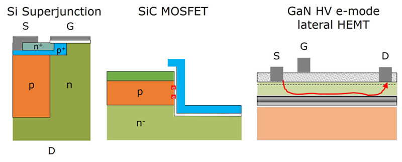
Figure 1: Comparison of Superjunction transistor, SiC MOSFET, and GaN HEMT
The commercial availability of Superjunction transistors 20 years ago, challenged and finally proved wrong the limitations of conventional silicon-based transistors with respect to on-state resistance. What was regarded as revolutionary at that time is standard today. Today there is not a single transistor from 25 V to 900 V in Infineon's portfolio that does not break the so-called silicon limit declared by Chenming Hu1 in 1978. Along with the Superjunction principle,2,3 field plate (or shielded gate transistor) concepts used for voltage classes from 25 V to 300 V similarly challenge the silicon limit.
These technologies today enable the use of MOSFETs across an extensive range of applications, from extremely low-power ones such as charging devices for cellular phones to rapid charging of electric automobiles from the 3-phase grid exceeding 100 kW of power. A key factor in the success of this class of semiconductors was the continuous reduction of the area-dependent on-state resistance, which coupled with the improvement in device characteristics, such as conductive and switching losses, reduced the costs per function even further with each technology generation.
As a consequence, it became possible to use power transistors with extremely low on-resistance in high-power applications such as AC/DC and DC/DC stages for server or telecommunications switch-mode power supplies. Efficiency levels of greater than 98% per stage or above 96% for single-phase power supplies (e.g., 3 kW, 12 V DC) are possible today with silicon technology.
What are hence the characteristics of wide-bandgap power devices that lead the power electronics industry beyond the established silicon technology?
Comparison of semiconductor characteristics
The key topic of providing ever-lower on-state resistance at a given breakdown voltage on an ever-smaller die size is achievable in various techniques. SiC MOSFETs, for instance, follow basically the same theorem as standard high voltage transistors; however, due to the very high breakdown field strength and the resulting possibility to handle high voltages on a reduced vertical distance, SiC can achieve theoretically up to three times lower Ron*A than conventional silicon transistors. GaN HEMTs, on the other side, are conducting via an undoped layer This conducting layer is typically referred to as two-dimensional electron gas or 2DEG. The physical behavior of this allows GaN HEMTs to achieve even lower Ron*A than SiC MOSFETs. Nowadays the Ron*A of SiC MOSFETs and GaN HEMTs in the 600 V and 650 V class respectively is two to four times lower than the best silicon-based technology available on the market.
Whereas Superjunction semiconductors and SiC MOSFETs employ vertical transistor concepts – i.e., the load current flows from the surface of the transistor vertically to the backside substrate, GaN HEMTs are lateral transistors. The source, gate, and drain terminals are all on the surface of the semiconductor and are connected via separate metallization layers. Figure 1 shows the corresponding semiconductor structures.
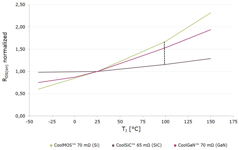
A first application-relevant parameter is the temperature dependence of the on-state resistance. While the scattering of carriers gives the temperature coefficient of Superjunction semiconductors on quantized lattice vibrations and doping atoms, the current in GaN HEMTs flows through a basically undoped, and therefore impurity-free crystal structure. For this reason, GaN HEMTs show very high mobility of electrons (HEMT stands for high electron mobility transistors) while their resistance has a lower temperature dependency than its silicon counterparts. Two overlapping effects can be observed in SiC MOSFETs: on the one hand, the rise in resistance of the drift zone with increasing temperature, which is however nearly fully compensated by improvements in the conduction characteristics of the MOSFET channel. This leads to a practically temperature-independent characteristic of the on-state resistance, in particular for the 600 V / 650 V voltage class with its relatively high contribution of the MOSFET channel resistance to the overall resistance. Figure 2 illustrates the corresponding comparison.
Click image to enlarge
Figure 2: Comparison of the on-state resistance as a function of the semiconductor temperature for Superjunction transistors, GaN HEMTs, and SiC MOSFETs
The characteristics of the channel also influence other relevant parameters, namely the gate charge and the gate voltage level, which are required for driving the transistor. GaN HEMTs are inherently self-conducting (special effort needs to be spent to realize a normally-off GaN HEMT) and therefore switch on with very low driving voltages. In contrast, SiC MOSFETs require a relatively high driving voltage due to the low charge carrier mobility of the MOS-channel. The reason for the low mobility is the relatively high defect density at the SiC/gate-oxide interface4; this effect is strongly evident in particular in lateral DMOS designs. For this reason, Infineon Technologies has chosen a trench concept in which the channel can be placed on a crystal plane with a considerably lower defect density.
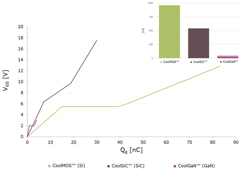
Along with improved transfer characteristics, this approach principally yields advantages in terms of reliability of the semiconductor since the electric field strength at the gate-oxide in the active state can be significantly lowered. Superjunction devices are due to their relatively long channel and the overlapping of the gate electrode with the n columns, at the upper end of the spectrum of the gate charge. In contrast to Superjunction transistors, GaN HEMTs with the same on-state resistance have with 5.8 nC a gate charge that is lower by more than one order of magnitude. Furthermore compared to SiC MOSFETs, the gate charge is still lower by a factor of 5. However, losses in the required RC driving circuit and a permanent gate current for concepts with bipolar gate structure must also be taken into account. When considering the overall driving power, a GaN HEMT requires an amount of power about one order of magnitude lower than that of a comparable SiC MOSFET. This is an important factor, particularly for high-frequency applications. Figure 3 shows a graph of the gate charge for the three examined semiconductor design concepts.
Click image to enlarge
Figure 3: Comparison of gate charge (Figure 3a) and driving power (inset, top right) of Superjunction transistors, SiC MOSFETs and GaN HEMTs (with and without losses in the RC circuit)
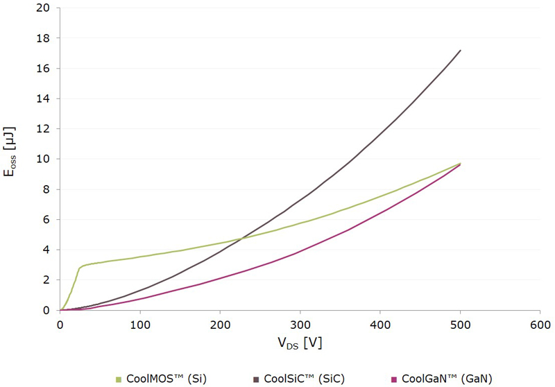
Besides the gate characteristics, the electrical behavior of the semiconductor when switching is primarily determined by the behavior of the output capacitance. The shallow high-voltage segment of the output capacitance of Superjunction devices and the resulting extremely low level of stored energy, Eoss, make them particularly suitable for hard switching. Due to the striking non-linearity of the output capacitance, the transistor can be switched off practically loss-free. The switching losses during hard switching are subsequently reduced to values close to the energy, Eoss, stored in the output capacitance. Particularly when combined with SiC Schottky diodes as a freewheeling element, an ideal semiconductor combination can be obtained that dominates today the world market for power factor correction circuits, which are compulsory for AC/DC power supply units from 75 W upwards.
As the comparison of Eoss energy values in Figure 4 shows, GaN HEMTs achieve the same level as Superjunction semiconductors. Nonetheless, silicon-based Superjunction transistors will already lead in this parameter versus GaN already in the next generation. We expect, therefore, that single-ended topologies such as the PFC stage will remain a key application for Superjunction devices.
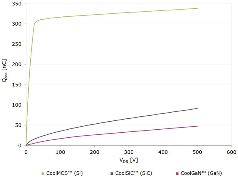
In contrast, wide-bandgap semiconductors will play to their full strength in half-bridge based topologies such as the totem pole for bridgeless PFC circuits. Here, both SiC and GaN can make full use of their strengths5. Of relevance here is, on the one hand, the reverse recovery charge Qrr – i.e., the charge stored in reverse operation of the semiconductor, and on the other hand, the charge of the output capacitance Qoss. In this regard, the GaN HEMT is almost an order of magnitude better than its silicon counterpart and a factor of 2 below SiC MOSFET.
Concerning Qrr, GaN shows clear benefits due to the complete absence of any stored bipolar charge. The reason for this is the absence of a pn junction in the semiconductor design, which could be forward biased in the case of reverse polarity operation. GaN HEMTs conduct in the reverse direction similarly to a lateral CMOS as soon as the drain voltage becomes lower than the difference between applied (negative) gate voltage and the threshold voltage. Although SiC MOSFETs have an integrated body diode that in principle injects bipolar charge in reverse operation, the ambipolar carrier lifetime is that short that only a minimal amount of Qrr can be seen outside the device at the terminals, even at fast commutation speeds. Figure 4 shows the energy stored in the output capacitor, Eoss, and the corresponding charge, Qoss, in comparison with all discussed semiconductor designs.
Click image to enlarge
Figure 4a: Comparison of the energy stored in the output capacitor, Eoss
Click image to enlarge
Figure 4b and the charge Qoss for Superjunction semiconductors, SiC MOSFETs, and GaN HEMTs
Performance in the switching power supply unit
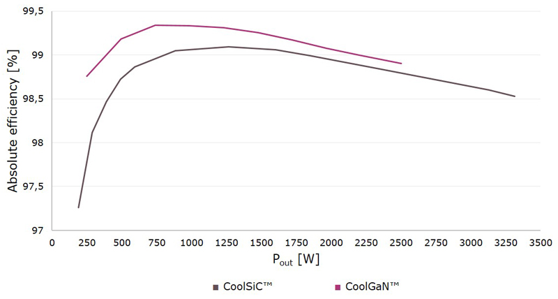
We compare all semiconductor designs in the power factor correction circuit mentioned above. The totem-pole topology is best suited for the wide-bandgap representatives. In this topology, one half-bridge with high switching frequency (45 kHz – 65 kHz) is connected directly to the AC mains via an input choke while a second half-bridge operating as synchronous grid rectifier, is connected with the neutral conductor. If a trapezoidal current characteristic (continuous conduction mode or CCM) is selected as the modulation method, a hard commutation event occurs in the high switching frequency half-bridge in every switching cycle. In this operation condition, SiC and GaN show their full benefits for Qrr and Qoss. Due to the lower Qoss values and the complete absence of the reverse recovery charge, the GaN HEMT in this comparison shows an advantage versus SiC MOSFET at an efficiency delta of about 0.1 % to 0.3 %. Both semiconductor technologies break through the magical barrier of 99 % efficiency, which is essential for SMPS targeting a total efficiency of 98%+. The semiconductors operate on two different test platforms; in the case of the SiC MOSFET, the operation frequency is 45 kHz, while the test platform for the GaN HEMTs operates at 65 kHz. The input AC voltage is 230 V AC.
Click image to enlarge
Figure 5: Efficiency of SiC MOSFETs and GaN-HEMTs in a totem pole PFC topology with trapezoid-shaped current modulation
Superjunction semiconductors cannot be used in this topology with trapezoidal current modulation due to the high reverse recovery losses. However, the triangular current mode (TCM) totem-pole PFC provides an alternative control method being compatible with Superjunction transistors and offers efficiency levels of 99% likewise. Nevertheless, the disadvantage compared to CCM operation wide-bandgap transistors is the increased complexity of the driving circuit due to variable switching frequency-changing across a wide span with load and AC input voltage. Furthermore, precise detection of the zero current crossings is required.
The use of Superjunction devices is particularly widespread in conventional CCM PFC stages with a bridge rectifier. Nevertheless, the H4 topology (a semi-bridgeless topology), which features two power devices being connected anti-serially, has established itself in the market in recent years. In combination with two Superjunction transistors and two SiC Schottky diodes, the topology can achieve a peak efficiency of about 98.8%.
Summary
The race to lead the field in the 600 V / 650 V semiconductor class stays exciting. Each of the Superjunction transistors, GaN HEMT and SiC MOSFET designs discussed in this paper has its particular strengths. The knowledge of the individual characteristics concerning the target application will be vital in deploying the best-suited semiconductor solution. Infineon Technologies will support all semiconductor technologies with a tailored portfolio of RDS(on) classes and packages.