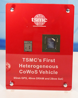
CoWoS includes SoC with Cadence Wide I/O memory controller PHY IP
Cadence Design Systems, Inc announcedthat TSMC has validated its 3D-IC technology for its CoWoS (chip-on-wafer-on-substrate) reference flow with the development of a CoWoS test vehicle that includes an SoC with Cadence Wide I/O memory controller and PHY IP. This is the foundry segment's first silicon-validated reference flow enabling multiple die integration, and features TSMC CoWoS and Cadence 3D-IC technologies to make 3D-IC design a viable option for electronics companies. ??The validated technologies in the 3D-IC solution span the CadenceEncounter RTL-to-signoff and Virtuoso custom/analog platforms. Also included are the Cadence system-in-package products and recently acquired Sigrity that helps engineers overcome die-stacking and silicon carriers' challenges from planning through implementation, test, analysis and verification. TSMC's unique CoWoS combo bump cells, which simplify bump assignment, are now supported automatically in the Cadence Encounter Digital Implementation (EDI) System, QRC Extraction, and Cadence Physical Verification System. The CoWoS Reference Flow is supported with a CoWoS design kit and silicon validation results from a TSMC test vehicle. ??TSMC chose Cadence's high bandwidth, low power Wide I/O controller and PHY Design IP solution to connect the SoC to Wide I/O DRAM using CoWoS technology featuring a peak data rate of over 100Gbit/sec for memory interface.?? 3D-IC technology offers several key benefits for engineers developing today's complex designs, including higher performance, reduced power consumption and smaller form factor. TSMC's CoWoS is an integrated process technology that bonds multiple chips in a single device to reduce power and form factor while improving system performance. Cadence 3D-IC technology enables multi-chip co-design between digital, custom and package environments incorporating through-silicon vias (TSVs) on both chips and silicon carriers, and supports micro-bump alignment, placement, routing, design for test, as well as analysis and verification from a system perspective. The Wide I/O controller and PHY demonstrate the advantages of implementing memory subsystems on 3D-IC technology for increased memory bandwidth with significant reduction in operating power. ??"The Cadence 3D-IC technology enables the next generation of high-performance mobile devices, and offers significant benefits in system performance and power efficiency," said Chi-ping Hsu, senior vice president, R&D, Silicon Realization Group at Cadence. "Our continued work with TSMC on the CoWoS process ensures that the infrastructure is in place to support this important emerging technology."?? "TSMC continues to work closely with Cadence to bring 3D-IC to the industry," said Suk Lee, TSMC senior director, Design Infrastructure Marketing Division. "We have invested three years with OIP ecosystem partners to prepare the CoWoS™ design flow for production, and now we're ready to enable customers' 3D-IC designs with TSMC CoWoS technology." Cadence Sigrity TSMC