Toshiba's latest automotive MOSFETs lower RDS(ON) by up to 22%
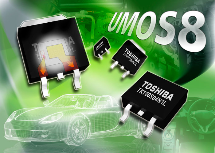
Toshiba Electronics Europe announced the first in a line-up of automotive MOSFETs that brings together the latest UMOS8 low on resistance (RDS(ON)), low input capacitance (Ciss) trench process with high-efficiency, high-reliability DPAK+ packaging. At just 2.4m?, the 40V, 100A TK100S04N1L has a maximum RDS(ON) that is 22% lower than previous devices with the same ratings. The new MOSFET is AEC-Q101-qualified for operation with channel temperatures up to 175°C and is ideally suited to automotive motion control applications including fans, pumps and brushless DC (BLDC) motors. Toshiba's eighth generation UMOS trench process delivers significant improvements in trade-off characteristics between RDS(ON) and Ciss, as well as improving switching speeds and minimising radiated noise. This process, combined with the proprietary �WARP' technology used in the DPAK+ package, allows the TK100S04N1L to offer a typical RDS(ON) of just 1.9m?. While offering the same form factor as, and pin-to-pin compatibility with, a traditional DPAK package, DPAK+ replaces conventional internal aluminium bond wires with copper clamps. This highly reliable mechanical connection is capable of withstanding repeated power cycling and exposure to shock and vibration. In addition, the large, cross-sectional area combined with improved electrical connectivity minimises heating due to package losses and reduces package inductance. This, in turn, lowers thermal losses and noise while supporting faster device operation. The TK100S04N1L has a maximum channel-to-case thermal resistance of 1.5°C/W and can handle a maximum pulse drain current up to 200A. Drain power dissipation at 25°C is rated at 100W while maximum leakage current (@ VDS = 40V) is an ultra-low 10μA. Following the introduction of the new 40V device, Toshiba plans to launch 60V and 100V automotive MOSFETs built around the same process and packaging technologies. Toshiba