Understanding Thermal Resistance's Impact at a System Level
True thermal performance of a device will depend more on the measures taken at the PCB level, rather than the junction-to-case figure in a data sheet
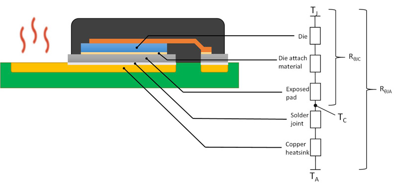
Figure 1: Thermal resistance comprises multiple stages, from junction to ambient
The principles that apply to current flow, in terms of resistance, can be likened to the resistance that heat encounters when flowing from hot to cold bodies. Every material and its interface will have a thermal resistance, and these figures can be used to calculate the rate at which heat is removed from its source. In an integrated device, the source of that heat is invariably the semiconductor junction, and allowing the junction to exceed its maximum operating temperature will lead to catastrophic failure. While there are techniques that integrated device manufactures use to design-in protection against this condition, such as over-temperature shutdown, they inevitably lead to disruption. A better solution is to make design choices that inhibit (or at least limit) the conditions that would result in the junction temperature exceeding its operating maximum. As a junction cannot be directly force-cooled, removing heat through conduction is the only way to ensure this. In order to achieve maximum design efficiency, engineers need to work within these limits.
Calculating the rate at which heat can be removed from a junction requires an understanding of the path the heat will take and all of the resistances it will encounter along the way. Figure 1 describes this, showing the path heat will take when flowing from the junction to ambient air. The total thermal resistance must include the thermal resistance of each material along that path. This highlights an important difference between two figures commonly used by device manufacturers: the thermal resistance from junction to case, RθJC, and the thermal resistance from junction to ambient air, RθJA. As Figure 1 shows, the figure for RθJA will include the figure for RθJC. Even though it falls outside the device manufacturer's control, characterizing their device under test conditions will provide the figure for thermal resistance to ambient as a guide for engineers using their device.
Measuring power dissipation as a function of junction temperature
The reason it is important to understand thermal resistance and how it affects a device is twofold. First, as stated earlier, it is important to keep the junction of a semiconductor below a level that would lead to failure. For most semiconductors based on a silicon process, this is typically 150°C.
Secondly, but closely related, is the fact that the junction temperature is proportional to the amount of power—or in simpler, terms, work—the semiconductor device can do while remaining below its absolute maximum junction temperature. Each time a MOSFET switches, it will incur a loss, which will generate heat. Switching at high frequencies will generate heat faster than it can be dissipated, resulting in an aggregate increase in junction temperature. The equation for calculating the power dissipated, as it relates to temperature, is shown in Equation 1, below.
PowerDissipated = Tj(max) - Tambient / Rθ
Eq 1
This equation will hold for whatever reference is used for the thermal resistance, Rθ. So, if the thermal resistance from the junction to case is used, the calculated power dissipated will be very different from that calculated using the thermal resistance from junction to ambient.
The amount of power dissipated by a device can also be calculated for a given application based on the current flowing through the device's junction and the junction's resistance. In addition, if the thermal resistance and maximum junction temperature are also known (taken from the data sheet) then simple transposition will give the value for the maximum ambient temperature permissible, indicating whether or not forced air cooling is required for the application.
Thermal resistance from case or ambient?
The potential for error is introduced here by the inconsistent way manufacturers refer to thermal resistance. As outlined earlier, the figure often used is RθJC, which does not take into account the thermal resistance between the case and ambient. This underreports the importance of the interface between the device's case and the rest of the system.
In terms of heat dissipation for a power MOSFET, the device's packaging will likely feature a large pad on the underside connected internally to the transistor's drain. This will be the primary thermal path to the device's junction, so the majority of heat generated at the device's junction will flow through the device and exit at this point. This pad will, in turn, be soldered to the PCB. As such, the size and shape of the PCB's pad, the number of layers and distribution of tracks all influence the rate at which heat can be dissipated to ambient through the PCB. This figure is much more design-dependent than the thermal resistance path inside the device, and it follows that the dominant figure in the thermal calculation is the resistance between case and ambient.
The importance of heatsinks in thermal management and junction temperature
This highlights the importance of heatsinks in a power application. Adding additional copper layers, or increasing the size or thickness of a copper layer will have an effect on the thermal resistance to ambient figure. One simple method for reducing the thermal resistance is to add or extend a ground plane below the power device. Another, more costly, solution is to add an external heatsink.
When considering the thermal management requirements for a power application, it is easy to make assumptions about those requirements based solely on the thermal resistance figures provided in the data sheet. To illustrate how this can be misleading, consider an example comparison between two power transistors. Both devices have similar parameters in terms of VDS, ID and RDS(ON). However, they use different packages, and one gives a thermal resistance to case, RθJC, of 1.0°C/W while the other states 0.5°C/W.
At first glance, it would appear that the device with a lower thermal resistance will operate at a much higher ambient temperature, potentially 50% higher based on the figures given. This could make the difference between needing an external heatsink or simply adding a larger ground plane. Clearly, the larger ground plane would be the lower cost option in terms of the bill of materials and manufacturing effort. However, as shown in Figure 2, which charts the actual thermal resistance to ambient for both devices, measured under equal test conditions and using copper pad sizes from 30 to over 300mm2, the actual difference is negligible.
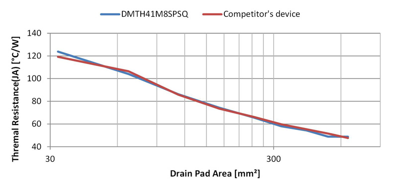
Click image to enlarge
Figure 2: The actual difference between RθJA for two comparable devices with significantly different RθJC values as given in their data sheets
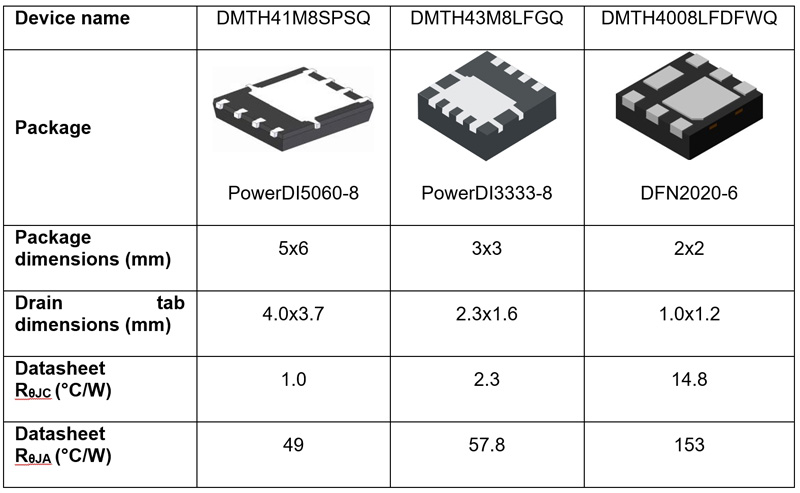
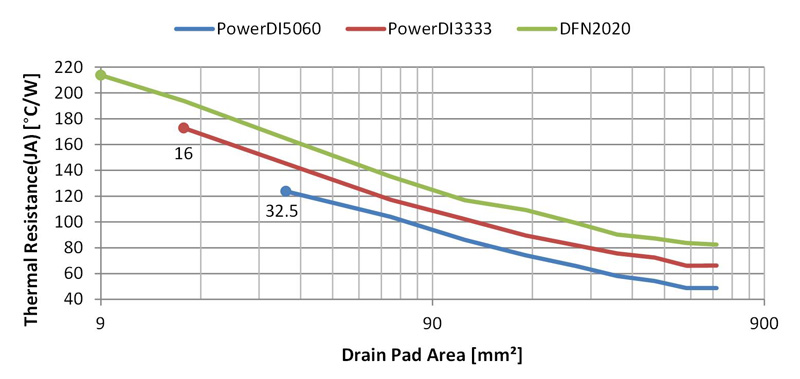
To illustrate this point, consider the devices shown in Table 1, which compares three power MOSFETs from Diodes Incorporated, each with significantly different thermal resistance figures. The graph shown in Figure 3 charts the thermal resistance of each device for various copper pad areas. The fact that all three lines describe a similar trend, even though they have significantly different junction-to-case thermal resistances, indicates the dominance of the PCB in defining the thermal resistance as measured from junction-to-ambient.
Click image to enlarge
Table 1: Three power MOSFETs from Diodes Incorporated, showing different thermal resistances
Click image to enlarge
Figure 3: The thermal resistance of three power MOSFETs from Diodes Incorporated
To meet demand from customers eager to develop compact and power-dense applications, more manufacturers are adopting smaller, surface-mount packages for power MOSFETs. This puts greater pressure on the designer, who has less freedom in product design. Identifying thermal resistances is crucial in developing products that include power MOSFETs in surface-mount packages as they will often be restricted in terms of additional thermal management measures, such as heat sinks or fans.
By understanding how thermal resistance paths are configured, from junction to ambient, and the important role the PCB plays in managing heat distribution, engineers will be able to make design decision based on their actual requirements, rather than artificial restrictions in power dissipation.
Conclusion
Dealing with the heat generated by devices such as power transistors is an important part of the overall design effort. The thermal resistance provided by a manufacturer is a convenient figure to describe the amount of energy that can be dissipated as heat by a device before it fails. However, it must be understood that the true performance will depend more on the measures taken at the PCB level, rather than the junction-to-case figure in a data sheet.


