USB Type-C Power Management Design for Portable Devices

Applications and portable devices with USB Type-C connectors have become increasingly common in recent years
Figure 1: O-Ring Circuit
Among the many benefits of USB Type-C connectors are their small size, easy-to-use features, and versatility. USB Type-C (also called USB-C) can support multiple protocols, such as USB 3.1, DisplayPort, HDMI, and USB PD. The USB Implementers Forum (USB-IF) released guidelines for USB Type-C called USB Type-C Cable and Connector Specification, which outlines the standards for USB Type-C to achieve their versatility. This article will discuss USB Type-C specifications, and recommendations for how to design a simplified power delivery solution that meets the necessary requirements for powering portable devices and accessory applications.
The USB Type-C specification defines four pairs of power pins to deliver power, and two CC pins to detect the device status. The USB Type-C specifications define two potential power sources: VBUS and VCONN. The VCONN pin does not have particular specifications, as it is always between 3V and 5V, but VBUS has a wide voltage range that must comply with a different protocol, such as USB PD. Under USB PD protocol, the VBUS voltage can be as high as 20V. To protect connected devices when the voltage suddenly rises, the USB Type-C Cable and Connector Specification requires that the pins connected to the VBUS pin can tolerate voltages up to 21V.
For electrically marked USB cables, both VCONN and VBUS can provide power. If VCONN is available and detected, the connected device is powered by VCONN. If VCONN is removed, the device is powered by VBUS. To monitor the availability of these power paths, the system requires an O-ring circuit to detect any power changes.
Figure 1 shows a traditional O-ring circuit. This circuit has four I/O pins, two power input pins (VIN1 and VIN2), one output power pin (VOUT), and a selection pin (SEL). When the SEL pin receives a signal, the internal logic controller generates two control signals to select the power path from either VIN1 or VIN2.
An example application for a USB Type-C cable is when VBUS is connected to VIN2, and VCONN is connected to VIN1. When Q2 turns on and Q1 turns off, a current (IS) is generated from VIN2 to VIN1 due to the MOSFET’s body diode. With this set-up, the VBUS voltage can be as high as 20V, which means any device connected to VIN1 could be damaged.
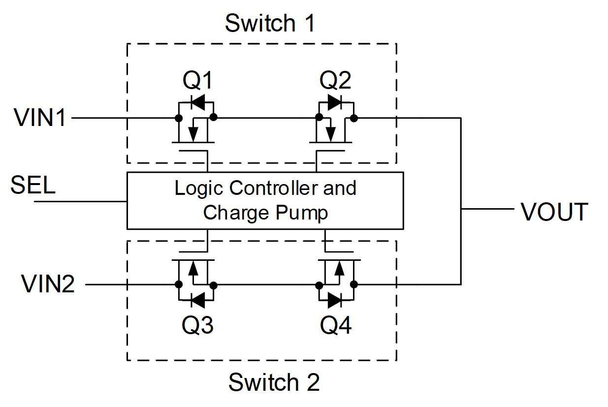
To solve this problem, an optimal O-ring circuit should be implemented using four MOSFETs (two paths with back-to-back MOSFETs) (see Figure 2). This circuit uses two MOSFETs as one switch. Because the body diodes of these two MOSFETs are in opposite directions, there is no leakage current if either switch (switch 1 or switch 2) turns on or off.
Using four N-channel MOSFETs (Q1, Q2, Q3, and Q4) to create two switches builds an O-ring circuit that can achieve fast transient for the two power supply pins (VIN1 and VIN2). The power supply path can be selected by the SEL pin.
Click image to enlarge
Figure 2: O-Ring Circuit with Back-to-Back MOSFETs
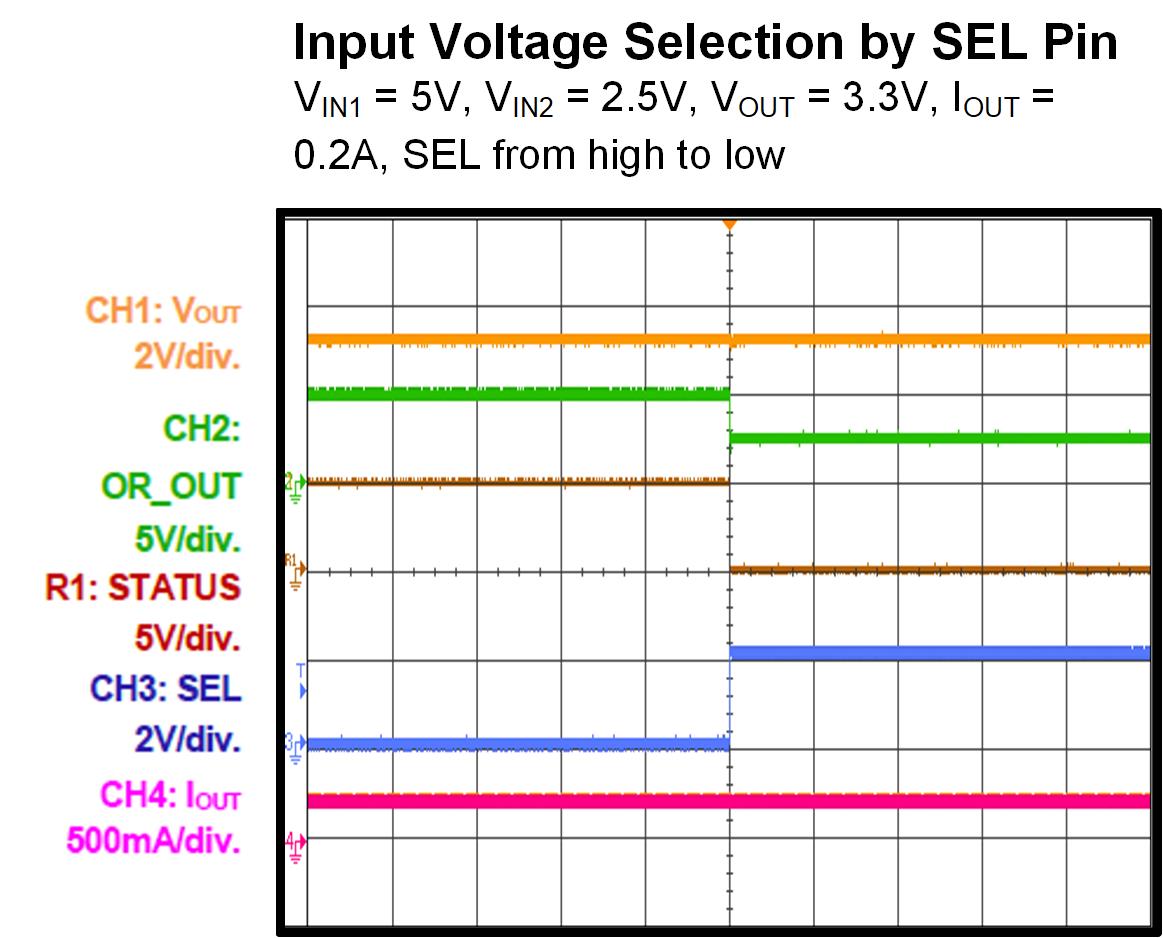
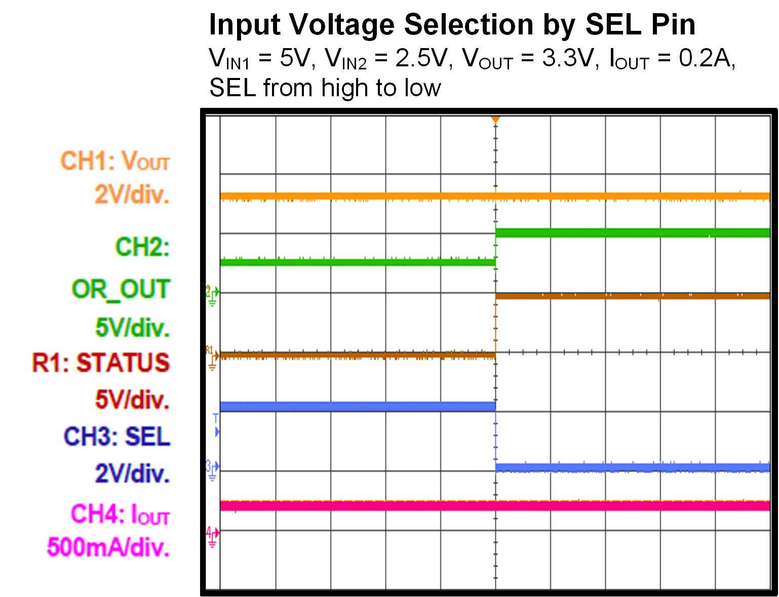
An example of a converter with this type of O-ring circuit integrated into its design is MPS’s MP5461, which provided promising results when tested (see Figure 3 and Figure 4). When the SEL pin switches from low to high and the supply pin switches from VIN1 to VIN2, VOUT maintains excellent output voltage stability without a high inrush current or voltage overshoot. The same goes for the switch’s supply pin when it goes from VIN2 to VIN1.
Click image to enlarge
Figure 3: Power Supply Changing from VIN1 to VIN2
Click image to enlarge
Figure 4: Power Supply Changing from VIN2 to VIN1
The USB Type-C Cable and Connector Specification clearly defines that the voltage range of devices powered by VCONN, as well as most electrically marked ICs, require either 3.3V or 5V. To guarantee a stable output, a buck-boost circuit is used to handle operation regardless of whether the input voltage is above, equal to, or below the output voltage. Using four MOSFETs to build a buck-boost circuit provides a greater transient response and high efficiency. To balance space and efficiency, two P-channel MOSFETs and two N-channel MOSFETs can be used to build a buck-boost circuit.
The USB Type-C Cable and Connector Specification offers a reference design for USB Type-C cables with very little space for electronic design. The most effective method to fit the design into a small space is to utilize a highly integrated power solution.
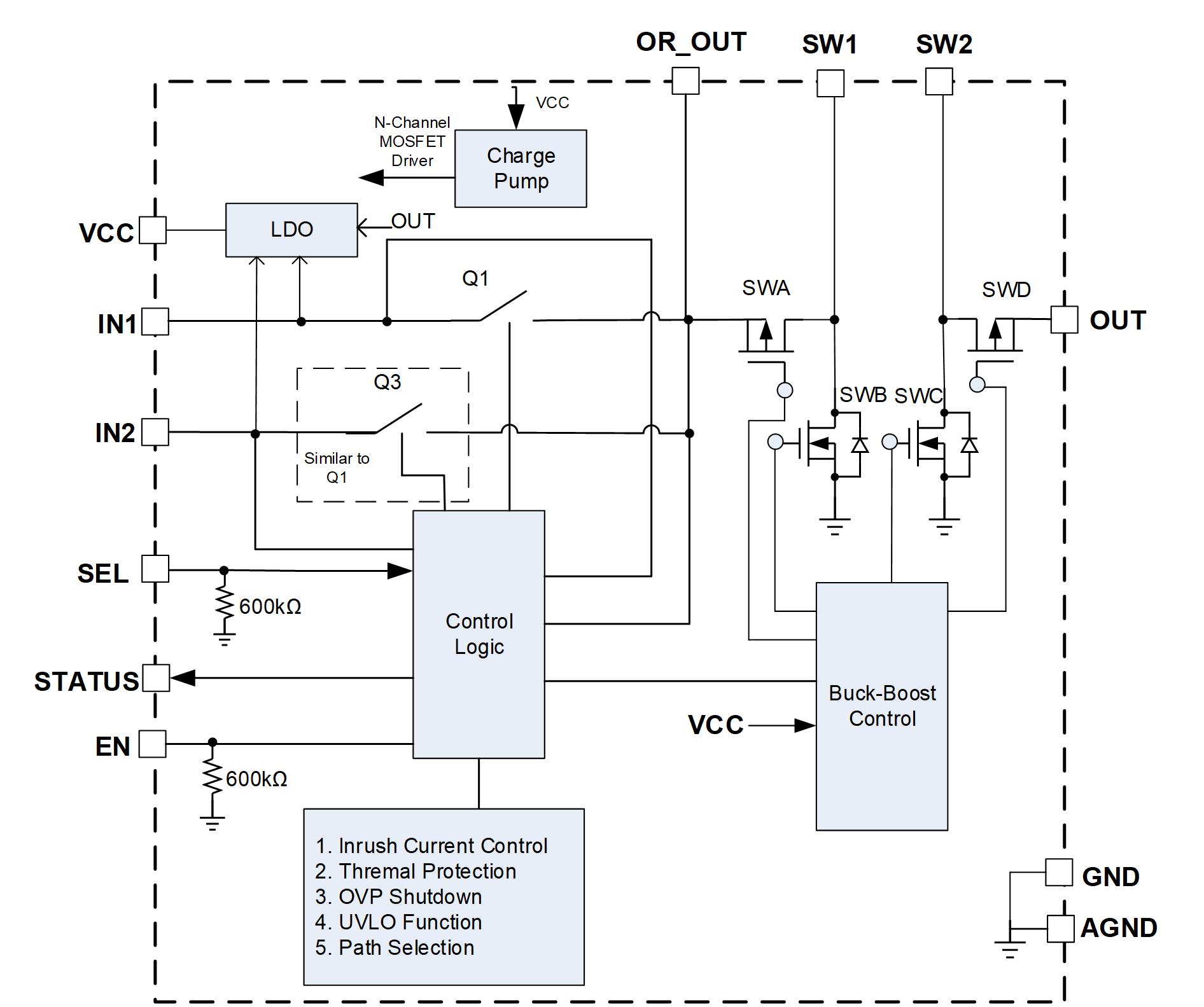
The MP5461 is one example of an efficient, space-saving power solution that meets these recommended conditions. Its integrated O-ring circuit is bolstered with four N-channel MOSFETs, as well as a buck-boost circuit with two P-channel MOSFETs and two N-channel MOSFETs, for a total of eight MOSFETs (see Figure 5).
Click image to enlarge
Figure 5: MP5461 Functional Block Diagram
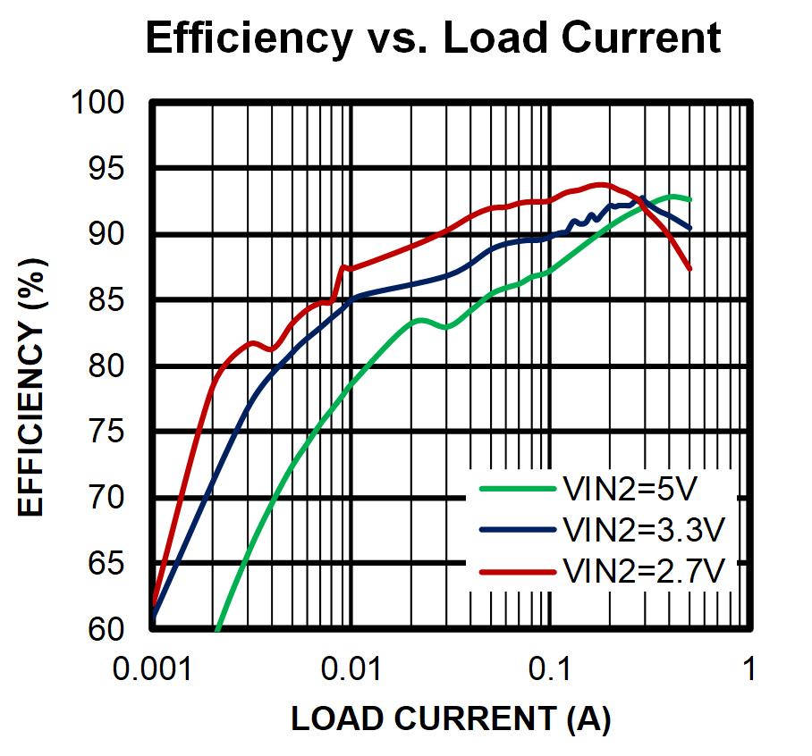
The device also provides power path management and a wide range of protections, including reverse current protection, over-voltage protection (OVP), over-current protection (OCP), thermal shutdown, and under-voltage lockout (UVLO). Housed in a tiny 1.4mmx1.8mm CSP package, it delivers up to 93.8% efficiency (see Figure 6).
Click image to enlarge
Figure 6: MP5461 Efficiency vs. Load Current
Conclusion
USB Type-C cables and connectors are small, but they are incredibly versatile and powerful, with a wide voltage range between two power sources (VCONN and VBUS). In order to have an elegant, compact design that can reliably handle and monitor USB Type-C voltages, an integrated power device with an O-ring circuit and a buck-boost circuit is strongly recommended. The circuit topology with its integrated O-ring circuit and buck-boost circuit is also suitable for multi-input power source applications, such as those with USB and battery input sources (e.g. Li-ion battery input). An ideal solution must be able to not only handle the two voltages effectively, but integrate the O-ring and buck-boost circuit into a single device to minimize board space and BOM cost. The high integration and built-in protections in the MP5416 make it a suitable and differentiated power device for accessory products with USB Type-C inputs, such as USB Type-C digital AV multiport adapters and USB Type-C to HDMI adapters.