The Kelvin Method lives on in the in the latest ultra-precise current-shunt monitors & current-sense amplifiers
Ultra-precision, high-side current sensing is crucial in applications where one must measure the current entering or leaving a battery. Today many digital multimeters feature four-lead Kelvin sensing to eliminate the series resistance of the multimeter leads and give an accurate voltage drop across a given resistor.
Similarly, a current-shunt monitor (CSM) or current-sense amplifier (CSA) measures voltage drop across a shunt resistor based on the current flown into or out of the battery. This is how you determine the amount of current drawn by the load from a battery in real-world applications. Systems today use low power and require a very accurate measure of charge left in the battery. To quantify remaining charge, every µA drawn from the battery by the load or pumped into the battery by a charger needs to be accounted for. Thus, ultra-precise sensing of voltage drop across the shunt is critical.
Let’s look at measuring voltage drop across a shunt resistor with very high precision. An ultra-high-precision CSM measures the voltage drop across the shunt resistor with typical connections, and then compares this value with the CSM accuracy specification in its datasheet. There are ways to improve the measurement accuracy using that same CSM.
These measurements are enhanced utilizing the proven Kelvin sensing methods with a four-terminal sense resistor. Test results also show that one should be careful with the board layout. Once the layout practices listed in this article are followed, we can capitalize on Kelvin sensing and sense the microvolt level drop across the sense resistor with ultra-high precision.
The Kelvin Bridge
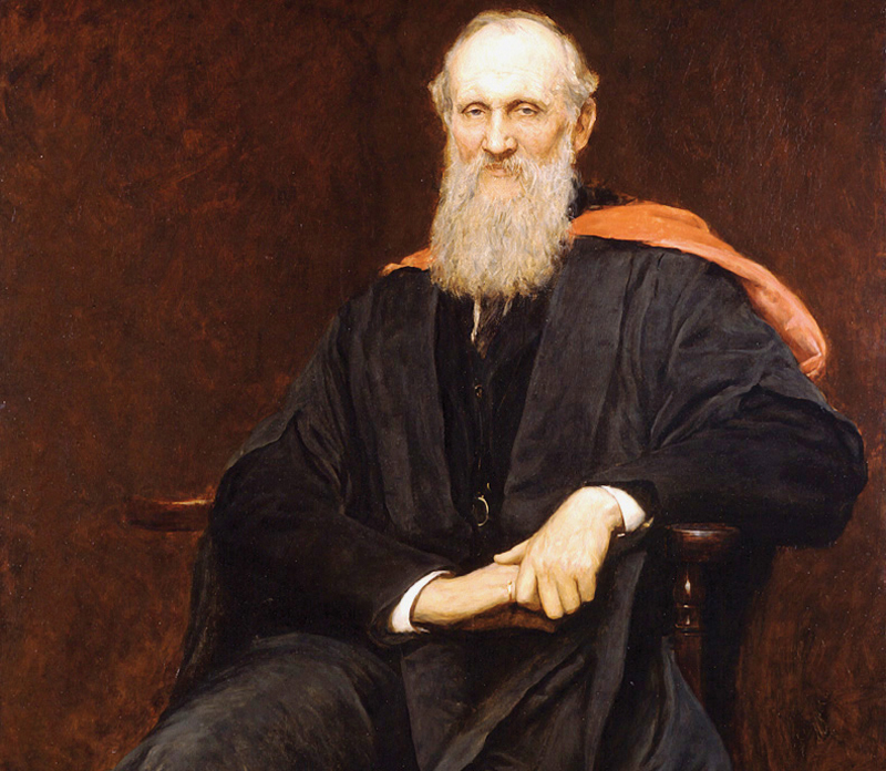
Before we talk about ultra-precision CSMs/CSAs, let’s start with a look back in time to an impressive scientist and Avant-garde engineer, Lord Kelvin (see Figure 1). Lord Kelvin’s pioneering effort is the basis of many electronic principles that we take for granted in our daily life, such as knowing when our cell phone needs charging. Kelvin’s work in measuring very low resistances is still used in modern integrated circuits (ICs). In fact, when you accurately measure battery capacity by applying early Kelvin principles and additional math, preventing overcharging or discharging extends battery life.
Clcik image to enlarge
Figure 1. A portrait of Lord Kelvin (1824-1907) by Sir Hubert von Herkomer (1849-1914).
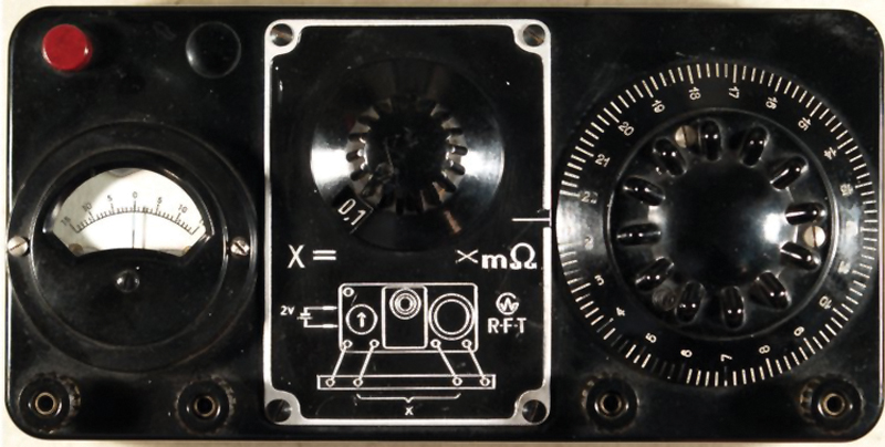
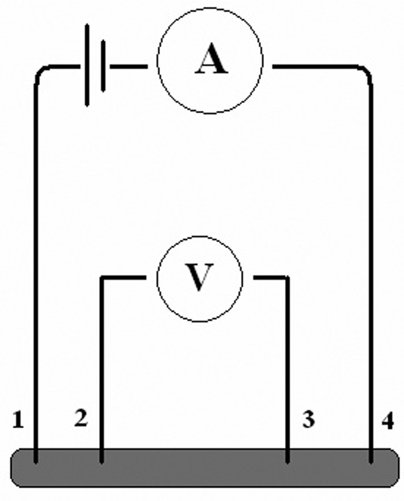
Early instruments such as the Kelvin bridge (see Figure 2) are amazingly accurate by today’s standards. Note the block diagram in the center of Figure 2. On the left is a battery and below are four leads. The outer leads supply current through resistor X, while the inner leads isolate the measuring circuit. It is easier to see the Kelvin sensing principle in Figure 3.
Clcik image to enlarge
Figure 2. An early Kelvin bridge for making accurate resistance measurements of very low-ohm resistors.
Click image to enlarge
Figure 3. A block diagram showing the Kelvin sensing method.
By separating the main current path from the measurement path, Kelvin improves measurement accuracy. In Figure 3, the main current to be measured flows from the battery on the top left through the ammeter (A), and the voltage drops across resistor “X” (the gray bar at the bottom) between leads 2 and 3. Virtually no current flows through the voltmeter circuit (V and leads 2 and 3) due to very high-input impedance and, hence, the voltmeter makes a highly accurate measurement. The current is the same at all parts of the main circuit comprised of the ammeter, battery resistor, and leads 1 through 4. However, the leads 1 and 4 contribute series resistance that, in turn, contributes to a finite amount of voltage drop along the leads. Although very small voltage drops, nonetheless, they reduce accuracy.
By separating the main current path from the measurement path, Kelvin’s sensing improves the accuracy of measurements. Of course, knowing any two of the three parameters—voltage, current, and resistance—we can calculate the third parameter.
Typical connections on a current-shunt monitor
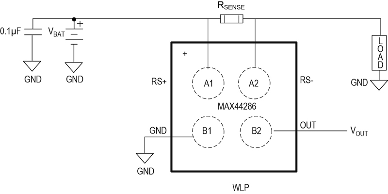
Figure 4 shows connections around a CSM used for monitoring current from the battery into the load. We might think at the outset that there is nothing wrong with Figure 4. However, this design will not yield the ±0.23% gain error specified for this CSA. The design problems actually result from shortcomings in the board layout and poor schematic placement.
Click image to enlarge
Figure 4. Typical connections to measure drop across a sense resistor. The example device serving as the shunt monitor is the MAX44286 CSA.
When we examine the schematic placement in Figure 4 and make some adjustments, we can preserve the shunt monitor’s DC accuracy parameters like gain accuracy and input-offset voltage. The example shunt monitor shown here is the MAX44286 available in a 4-bump wafer-level package (WLP) with 0.78mm x 0.78mm x 0.35mm dimensions. These findings and recommendations will apply similarly to any precision CSA. Although our analysis here is done with the MAX44286, the results are true and should hold good for any high-precision CSMs.
We begin the analysis of Figure 4 with a well-known axiom:
VOUT = Gain × VDIFF
Where:
•VOUT is the amplifier’s output on bump B2 in volts.
•VDIFF is input differential sense voltage in millivolts due to the current flow through shunt resistor RSENSE placed across the inputs.
•Gain is inherent to the amplifier based on the gain option chosen (for example, 25V/V, 50V/V, 100V/V, 200V/V).
Gain accuracy or gain error is a critical parameter in precision applications where highly accurate sensing is needed on µV-to-mV level drops across a sense resistor.
Therefore:
Gain Error (GE) = [(GainMEAS – Gain IDEAL) × 100]/GainIDEAL
Where:
• Gain error is the percentage deviation between the observed differential gain and the ideal differential gain expected of the CSM.
• GainMEAS is the gain achieved in V/V.
• GainIDEAL is the gain that the device is rated to provide in V/V.
Below are the results for the MAX44286 on bench tests for the setup in Figure 4. To read the most accurate measurement of voltage drop, we calculate gain error by a two-point differential voltage covering both extremes of the full-scale differential sense range. Our test conditions were VBAT =5.5V with GIDEAL = 50V/V version at room temperature.
Specifically:
• VDIFF = 60mV, 4mV as two points
• VOUT with respect to GND = 2.99264V, 0.1992298V, respectively
• GMEAS = VOUT/VDIFF
So, calculating gain error per Equation 2 yields:
Gain Error (GE) = -0.23713148%
Now this result is not what we expect from this CSM, as its maximum gain error spec is ±0.23%.
Another important specification in these ultra-precision sense amplifiers is input offset voltage, given by:
VOS = (VOUT - VDIFF × GMEAS)/GMEAS
Where:
VOS is the CSM’s input-offset voltage specified in microvolts due to mismatch in the input pair. From Equation 3 and our test results, we achieve:
VOS = -5.93281µV
Gain Accuracy and input VOS of CSA improve with a Kelvin sensing layout
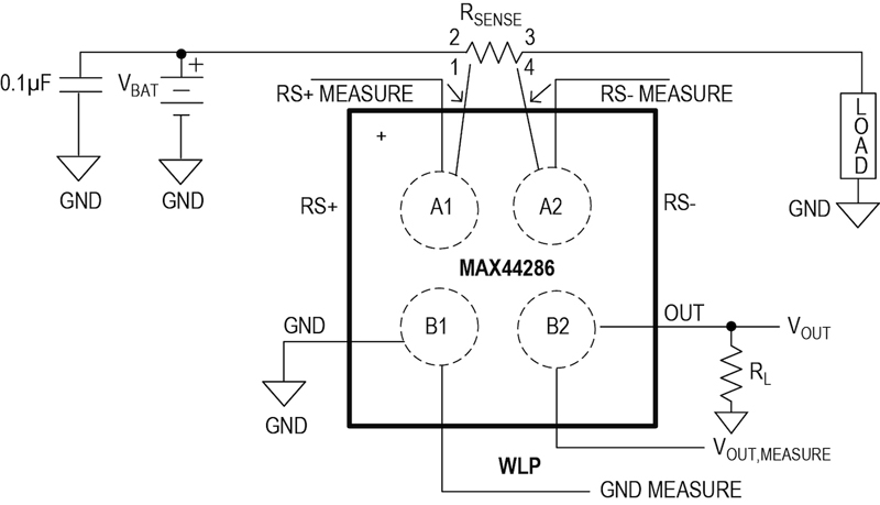
There is a way to achieve gain error that is always less than ±0.2%, and better input-offset voltage. Examine Figure 5 and notice that there are a few more traces than in Figure 4.
Click image to enlarge
Figure 5. Circuit shows Kelvin connections on both inputs, output, and ground bump. Once again the MAX44286 is the example CSA acting as the shunt monitor.
Traces from the sense-resistor terminals to the amplifier inputs carry input bias current. Supply current to the amplifier is part of the input bias current drawn through the RS+ pin because there is no dedicated supply voltage pin on the MAX44286. Otherwise, the input bias current flows through the RS+ and RS- pins and the supply current flows through the VCC pin, if there is a dedicated supply pin. Also, this current through the RS+ bump increases as the input differential voltage increases.
Trace impedance will create a drop due to this current flow through the trace. The result will be extra gain error if the input sense voltage is calculated across the sense resistor, since we did not account for loss along the trace. These extra traces at the input bumps, RS+ MEASURE and RS- MEASURE, will have no effect on the input sense voltage when it is measured across them.
Note also that the extra GND MEASURE trace is isolated from the currents flowing to the board’s ground and is solely used as a ground reference for accurate output voltage measurement. Another trace coming from the OUT bump, VOUT,MEASURE, is isolated from the actual output trace carrying the load current when the load resistor sources or sinks current out of the amplifier. This isolation lets us accurately measure the output voltage at the OUT bump with respect to the GND MEASURE trace. From all this we can calculate the gain error and input VOS of the CSA very precisely.
If you notice, there is a four-terminal resistor used in Figure 5. The 4-lead Kelvin configuration enables current to be applied through two opposite terminals; a sensing voltage is measured across the other two terminals. This design eliminates the resistance and temperature coefficient of the terminals for a more accurate current measurement. Also, traces from the sense-resistor terminals are taken directly underneath the pads of the resistor, thus preventing any additional trace impedance on the sense resistor.
The results below were achieved on the bench with the setup shown on Figure 5.Gain error is calculated similarly where a two-point differential voltage covering both extremes is applied to the shunt monitor and the output voltages recorded. Our test conditions were the same as earlier, VBAT =5.5V with GIDEAL = 50V/V for the CSA at room temperature. Therefore, VDIFF = 60mV, 4mV as two extremes.
Now VDIFF is the input differential voltage measured between RS+ MEASURE and RS- MEASURE. Also the VOUT,MEASURE values, with respect to the GND MEASURE for 60mV and 4mV input sense voltages applied, are 3.013034V and 0.2141941V respectively.
Thus:
GMEAS = VOUT/VDIFF
So, calculating gain error from Equation 2 yields:
Gain error = -0.08518056%
Substituting VOUT,MEASURE calculated with respect to GND MEASURE and substituting yields:
VOS = 3.54415µV
We can clearly see that there is an appreciable change in the gain error and input VOS. Thus, preserving the ultra-precise measurements of a CSA depends on the layout and component placement on the test fixture. If we use the sensing traces to measure as shown in Figure 5, measurements are very accurate. In ultra-precision applications, sense voltages on the order of microvolt are very important for sensing current on the order of microamps. Clearly, each trace must be laid out with great care.
Traces from each sense-resistor terminal to the respective input bumps need to be symmetrical in shape and length. Having a 2-terminal sense resistor will also provide good gain accuracy readings within a maximum of ±0.23% over temperature. For more accurate results over temperature, use 4-terminal sense resistor.
Thus, we complement Lord Kelvin’s sensing principles by preserving the DC accuracy of an ultra-precision CSA. Precision measurements not only depend on the good design and layout of the CSA itself, but on the board layout as well.