Author:
Alfredo Ochoa, Product and Applications Engineer Manager at ProTek Devices
Date
07/01/2021
 PDF
PDF
Click image to enlarge
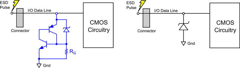
Figure 1. On the left is the TSPD functional model and, on the right, a TVS diode
With low-power, high-speed data systems, standard TVS diodes are commonly used in combination with low capacitance diodes to reduce the parasitic capacitance in applications like HDMI 2.0, USB 3.1, and Gigabit Ethernet. TVS diodes have offered the smallest form factors possible without sacrificing performance. But as circuit density continues to grow, the circuit protection industry needs a shift in solutions.
The advent of more data hungry applications is at the heart of circuit density growth. As a result, in recent years, hardware ESD transient protection solutions have also emigrated to higher frequencies of transmission. Here, circuitry is becoming more and more dense in the number of circuit elements. This is making them more susceptible to physical damage caused by electrical overstress. This push in the size reduction and increase in density is what is fueling demand for alternate circuit protection solutions.
There is one solid state technology that has been more focused in the telecom overvoltage circuit protection space. It is one particular thyristor structure known as a Transient Suppressor Protective Device (TSPD). The model is based on a typical SCR which consists in a P-N-P-N structure. This is where the gate current is controlled by an avalanche junction device (TVS diode) and a shunt resistor between the base and emitter of the NPN section (see fig 1).
There is an inherent advantage in this new thyristor device, as is being shown in the following diagram, which is compared to a TVS diode (see fig 2.)
Click image to enlarge
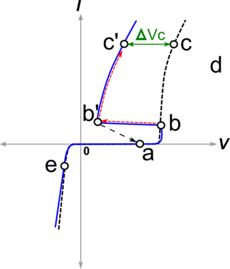
Figure 2. V-I characteristics comparing both devices
Getting into the Advantages
Black dashed trace plot – The TVS
The point “a” shown here is the point where the maximum peak operating voltage of a data signal line is. So, as long as this value is below the breakdown voltage (point “b”) the device will be in an off-state condition.
With a TVS device, if there is a case of an ESD event or a fast voltage transient, the device will “clamp” and follow the trajectory “b-c,” illustrated in figure 2. This will shunt the transient energy to ground and, after the transient is gone, the device will go back to the off-state again. As a unidirectional device, when it is biased in forward, the TVS behaves like a standard P-N junction with a VF at point “e.”
The Blue Solid Trace Plot for the Thyristor
In the same situation, for the blue line in figure 2, where point “a” is the operating voltage, we are now looking at a thyristor instead of a TVS. So, the ESD or fast voltage transient in the device “clamps” in the usual way as a TVS. So, it can reach a level where there will be enough current to initiate the conduction on the NPN transistor base. This will latch the device going on the trajectory “b-b’-c’” and will shunt all the energy to ground. After the transient is gone and the current drops below the holding current or goes to zero, the device will recover to the off-state. Here, it will follow the trajectory “b’-a.”
As is noticed, comparing both V-I curves, it is evident that there is a delta on the “Vc” at the same current (c vs. c’). This gives an extra layer of protection. It is also a less stressful situation to the CMOS circuitry of the application.
Transient Comparison
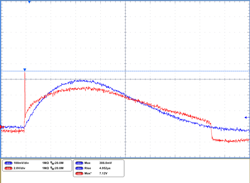
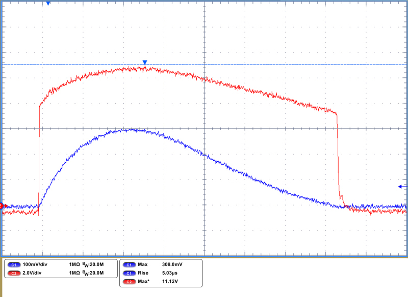
To give a physical example of this performance and the advantage of the thyristor structure versus the standard TVS diode, review figure 3 below. It shows both voltage and current wave plots under a surge pulse of 3Apk.
Click image to enlarge
Figure 3a. Thyristor Device under 8/20µs 3Apk
Click image to enlarge
Figure 3b. Std TVS Diode under 8/20µs 3Apk Surge
Click image to enlarge
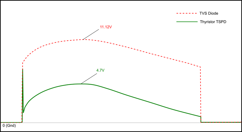
Figure 3c. Comparative voltage wave plots of both technologies together
Figure 3. Comparison of the Thyristor technology vs the standard TVS diode
Benefits
As is illustrated, a new incursion of this old technology into ESD and fast transient circuit protection provides a lower clamping voltage compared to the standard TVS structure. This will minimize stress to the application, keeping the voltage lower or to a minimum, to the tolerance on the voltage signal.
Also, the design of this small thyristor devices allows you to drop down the capacitance value to less than 0.35pF. This is compared to TVS diodes combined with low capacitance diodes of 0.5pF. So, this makes them suitable to operate in high-speed data signals up to 3GHz. As a result, there is greater application reach.
Since the thyristor device offers a lower clamping voltage, this implies it dissipates less power. Thus, it also improves overall design opportunities by reducing the die size area. It allows a design into smaller packages.
There are several advantages to point out. There is the intrinsic benefit of a lower clamping voltage and ultra-low capacitance. But it can also be packaged in single and integrated versions. In this way, thyristors can protect not only one but up to four or six data lines using the same form factor packages as existing TVS array solutions.
New Generation of Devices
Solutions using these thyristor-based devices can be implemented using rail to rail PCB mountings. This includes in spaces from 0.6x0.3 sq mm for a single bidirectional device or up to 1.3x0.8 sq mm in a quad integrated array. This minimizes parasitic impedance when re-routing trace lines.
Circuit protection technology solutions are advancing along this path. They need to in order to address growing circuit density. Solutions will likely be introduced or are already have been for such thyristor technology.
The thyristor represents a new generation of ESD transient protectors. They are ideal moving forward for engineers to design circuit protection into high current applications and high-speed buses like USB 3.1, HDMI 2.1, e-SATA and Gigabit Ethernet.