Variations to Perform: Introducing 65 W USB-PD Designs
Infineon solutions enable cost-performance, increased power density, and faster time-to-market
The continuous demand for charging devices in the shortest time is driving the charger market toward fast charging. On the one hand, the power delivered by these charges increases; on the other hand, their size is getting smaller and smaller, so it is necessary to design a higher power density. To meet the growing demand, Infineon has developed several solutions to meet cost and performance requirements. This article introduces different solutions that help engineers reach their design targets, whether it's cost-performance, efficiency, or ultra-high power density. We discuss the cost-performance champion PAG1 65 W, a high-density forced frequency resonant (FFR) 65 W, and an ultra-high-density hybrid flyback 65 W designs.
When cost-performance is the priority: the PAG1 65 W solution
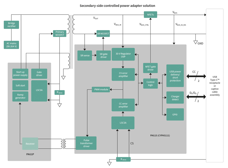
PAG1 is a two-chip USB-C power charger solution that comprises a primary start-up controller PAG1P and a single chip secondary-side controller PAG1S. PAG1P and PAG1S together operate in a secondary-side controlled flyback architecture.
In this design, the regulation happens on the secondary side with PAG1S, and the primary controller (PAG1P) acts as a simple gate driver. This combination achieves isolation between the primary and the secondary sides using a pulse transformer. The "brain" of the converter sits on the secondary side (PAG1S), where all decisions related to output voltage regulation are made, making the control loop faster. This architecture also enables immediate reaction to any fault on the secondary side, making the system more robust. By not using an optocoupler, the system behavior is more consistent and predictable from unit to unit over operating point, temperature, and product life.
Secondary-side controlled architecture also enables us to directly control the SR FET so that we can get ZVS (zero voltage switching). ZVS gives better efficiency on an existing converter without the use of any extra circuitry. With the ability to support higher loop bandwidth and faster dynamic response times, secondary-side controlled architecture is best suited to support higher switching frequency leading to high power density designs. However, one issue with this architecture is the initial power-up of the secondary side, necessitating the need for an extra auxiliary supply. This problem is solved with the use of the PAG1P. PAG1P helps power up the secondary side during startup. Once the system reaches the steady-state operation, it transfers the control to the secondary side and acts only as a primary-side gate driver with primary-side fault protection (OVP, UVP and OCP).
PAG1S is a programmable device and offers great flexibility in designing the power adapter. The user can fine-tune the QR valley at which the converter switches across line/load voltages and thereby can optimize the system efficiency without changing the external hardware components. The EZ-PDTM configuration utility tool allows the user to easily fine-tune the current sense resistor's value to account for the variations seen due to board designs without changing the hardware. The tool also offers the flexibility to configure the fault protection thresholds and the recovery mechanisms for overcurrent protection (OCP), overvoltage protection (OVP), short-circuit protection (SCP), and over-temperature protection (OTP). In addition, the PAG1S can be re-programmed on the field to cater to the latest USB-C PD standards or to address any possible post-production bugs.
Click image to enlarge

Click image to enlarge
Figure 2a & 2b: A 65 W reference design using the PAG1S and PAG1P in a 52 mm x 42 mm x 22 mm board
Having the arrow-eye on efficiency: the forced-frequency resonant (FFR) 65 W design
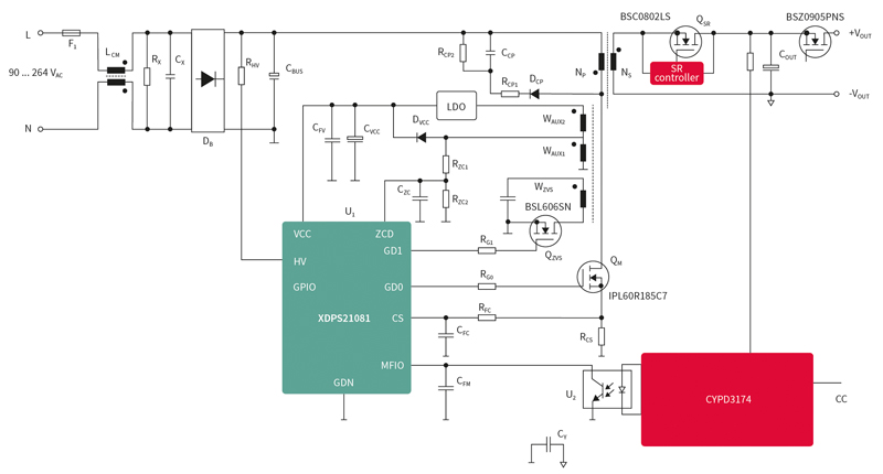
The solution accepts a wide input range from 90 VAC to 265 VAC, and the output is variable from 5 V to 20 V, the maximum output power is 65 W. The flyback topology and commodity components are selected to balance cost, performance, and production. Zero voltage switching (ZVS) is enabled with an additional ZVS winding and ZVS circuit driven by the PWM controller XDPS21081 GD1 pin.
Click image to enlarge
Figure 3: The forced-frequency resonant (FFR) 65 W USB-PD charger block diagram
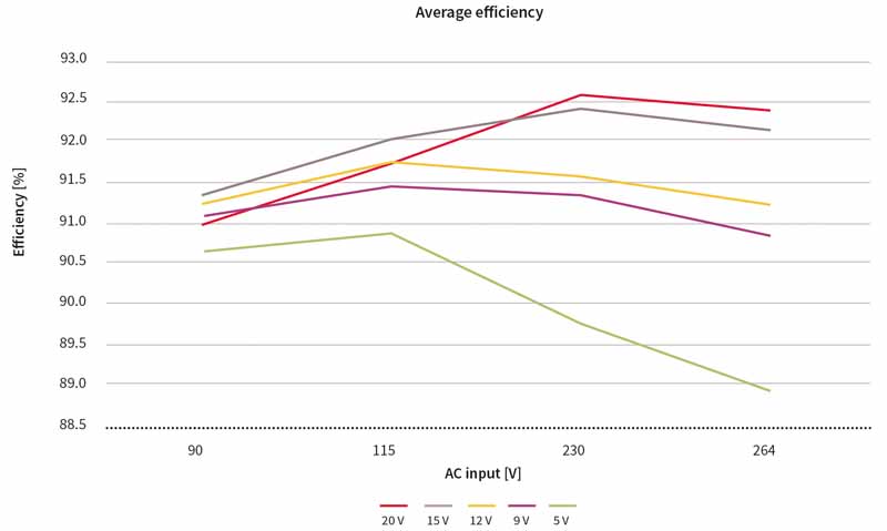
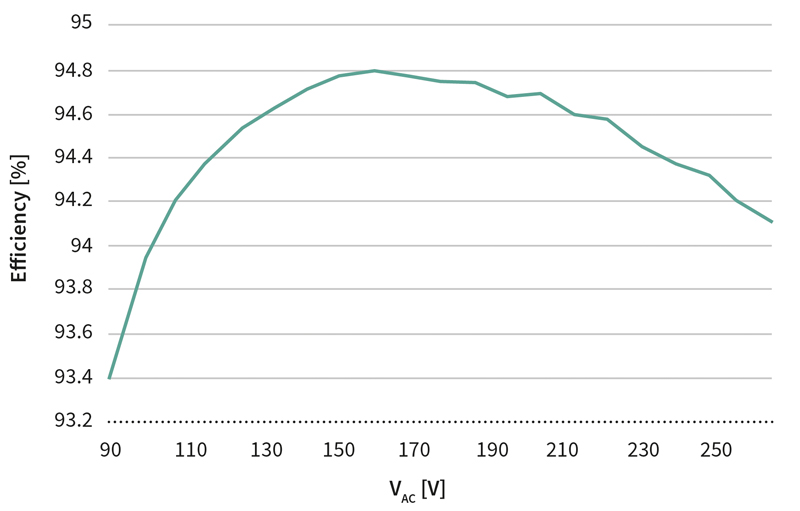
With the ZVS feature, the switching loss is significantly reduced at high-line so that the switching frequency can be set at around 140 kHz. The system will run in quasi-resonant (QR) with a heavy load for low-line, giving a natural ZVS effect to save power loss. Frequency reduction mode (FRM) and active burst mode (ABM) are implemented to keep high efficiency during medium loading and light loading. Figure 2 shows efficiency under different conditions.
Click image to enlarge
Figure 4: Four-point efficiency, surpass regulation requirements
Developed to perform in flyback: the forced-frequency resonant (FFR) flyback control principle
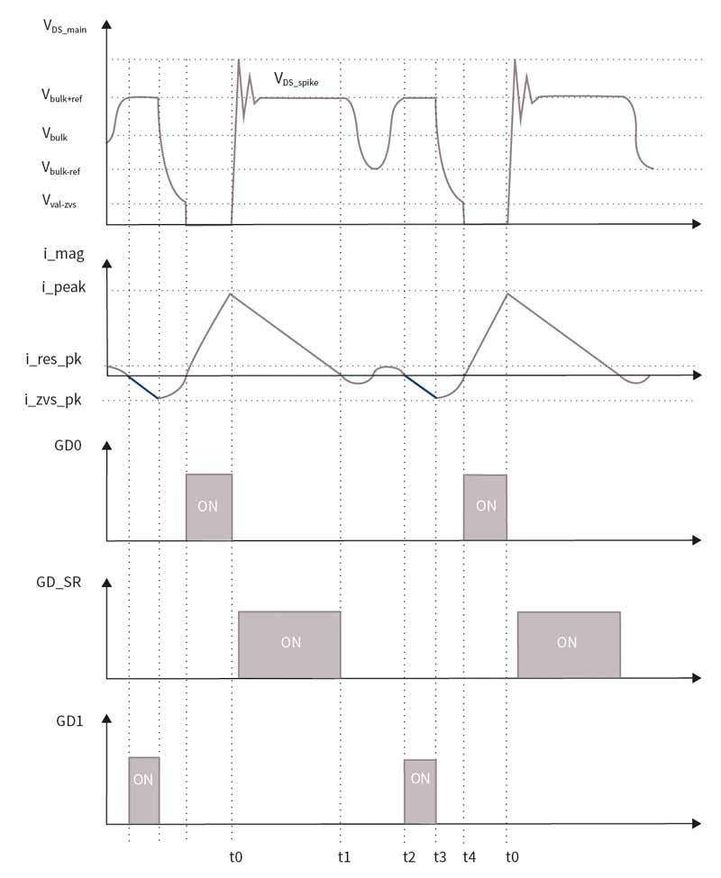
To optimize performance in a flyback configuration, Infineon has introduced the so-called forced-frequency resonant (FFR) flyback. It has several outstanding performance characteristics, including but not narrowed down to zero-voltage turn-on, fewer external components, or smaller difference in frequency during high- and low line input operation. (Figure 5 shows the topology and ZVS operation principles.)
After the primary MOSFET turns off at t0, the synchronous rectifier (SR) MOSFET will turn on, delayed by a short blanking time. At t1, the SR MOSFET turns off when the demagnetizing current ideally goes to zero, then the magnetizing inductance Lp and Ceqv will oscillate. The voltage of the primary MOSFET will oscillate from Vbulk+Vref to Vbulk-Vref. If the auxiliary MOSFET is turned on at t2, the primary MOSFET's resonant peak will mean the magnetizing current is zero; then the i_mag will build up as negative. During this controlled ZVS on-time, the Vds of the primary MOSFET is clamped to Vbulk+Vref. Once the peak current reaches i_zvs_pk, the aux MOSFET is turned off, and because this current is stored in the magnetizing inductance and in the reverse direction, it will continue to flow in this direction and discharge the energy stored in Ceqv. This time duration in the IC is controlled by the tZVSdead parameter, which is configurable. At t4, the primary MOSFET's drain voltage reaches its minimum and turns on the primary MOSFET, which reduces the turn-on losses significantly, which is almost ZVS. As seen in the diagram, the energy is proportional to Vbulk, and so is the ZVS on-time.
The ZVS pulse insertion is based on nano-DSP core and memory info. The IC knows the next switching cycle period and ZVS dead-time and ZVS pulse on-time, so the switching period minus these two parts will decide the ZVS pulse starting point, assuming the IC main gate turn-on time is also fixed. When the CS signal reaches the current command, the main gate off-point can also be decided.

Click image to enlarge
Click image to enlarge
Figures 5a & 5b: The topology (a) and the ZVS operation principles (b)
Achieving ultra-high-density: the 65 W design based on hybrid flyback control
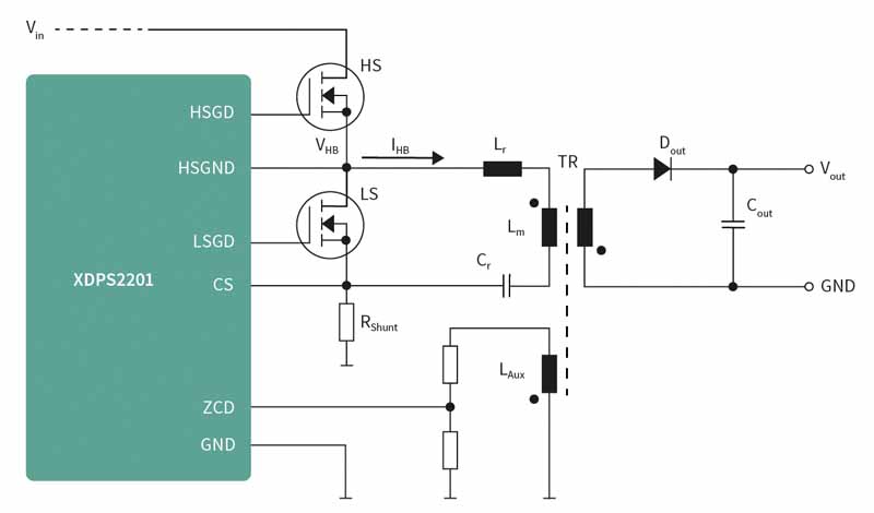
Infineon has introduced a new topology named hybrid flyback (shown in Figure 6), which is based on an asymmetrical half-bridge control. The half-bridge is driving a conventional flyback transformer in conjunction with a serial capacitor. The main inductances of the flyback transformer and the serial capacitor are building a resonant tank, which is used to achieve a ZVS behavior of the half-bridge power switches and is providing a resonant power transmission during the conventional demagnetization phase of the flyback transformer. During normal operation, the charge period and associated power is controlled by direct peak current control. In contrast, the demagnetization phase is timing controlled to ensure proper negative pre-magnetization required for a ZVS condition at the half-bridge power switches.
Click image to enlarge
Figure 6: Simplified schematic of an asymmetric half-bridge flyback
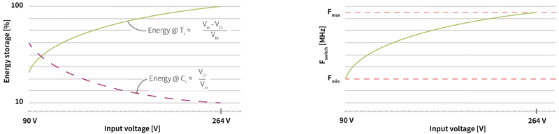
The power circuit in the primary side is realized via an LC tank driven by a half-bridge - similar to an LLC converter. The resonant inductor Lr represents the series inductance, Lr being either the transformer leakage inductance or the leakage inductance plus an external inductor, Lm represents the transformer's main inductance. The same converter can also be realized by connecting the resonant capacitor Cr and the primary coil of the transformer between the positive node and the middle point of the half-bridge. When the high side switch (HS) turns on, the energy will be stored in Cr and Lm; and the respective stored energy will be changing with input voltage and switching frequency (shown in Figure 7).
Click image to enlarge
Figure 7: Energy storage distribution and frequency variation diagram
When the high side switch (HS) turns off, the current in the transformer will force the half-bridge middle point (VHB) to drop until the body diode of the low-side switch clamps the voltage. Then the low-side switch will be turned on at zero voltage; at the same time, the transformer phase is reversed, and energy is transferred to the secondary side. When the low-side switch turns off, the negative current induced in the transformer during the previous phase will force the half-bridge middle point (VHB) to increase its voltage until it is clamped by the body diode of the high-side switch (HS). Similarly to the former phase, HS is switched on with the ZVS condition, and the LS is switched off. The current in the transformer's resonant tank is still negative, meaning that the excess of energy in the tank will be channeled back to the input.
Compared to other flyback topologies, less energy needs to be stored in the hybrid flyback transformer, thus reducing the charger size.
The hybrid flyback can achieve full ZVS operation on the primary and full ZCS operation on the secondary side, and the leakage energy is recycled. Thus high efficiency can be achieved.
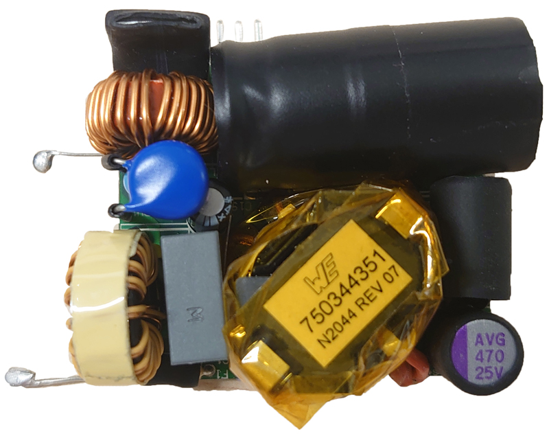
The dimensions of the final converter (see Figure 8a) are 51.5 mm x 38 mm x 19 mm. It achieves a power density of 29 W/inch3. The prototype achieved a minimum efficiency of 93.4 percent at 90 VAC input and 65 W load measured at board connectors.
Click image to enlarge
Click image to enlarge
Figure 8: Infineon's 65 W high-density design
Summary
Click image to enlarge
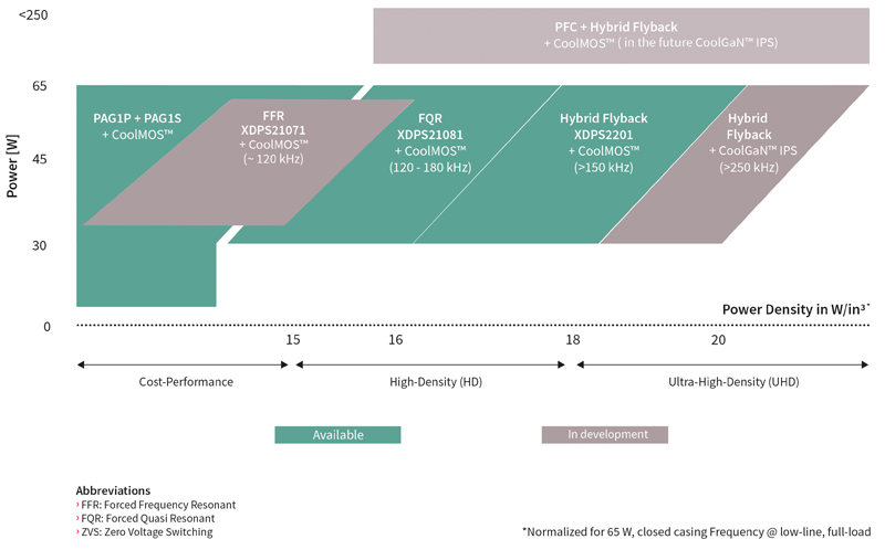
Figure 9: A comprehensive offering from Infineon to meet various requirements for USB-PD designs
Infineon's comprehensive portfolio enables high-density USB-PD charger designs by balancing cost and performance. Through the above-described different combinations, the high degree of differentiation of chargers is apparent. Infineon offers this variety to help design engineers and charger manufacturers to keep up with the latest technology trends, increase their competitiveness and reinforce their market position.
To discover more about Infineon's USB-PD charger solutions, please click here.
* The demonstration board will be available soon.
USB PD online training: “Fast charging solution with XDPS21081”
Application note USB PD reference design: “65 W USB-PD SMPS reference with XDPS21081”