When Does it Make Sense to Switch Out Si for SiC?
As SiC becomes more attractive for lower voltage applications, designers need to know when Si MOSFETs should make way for this new technology
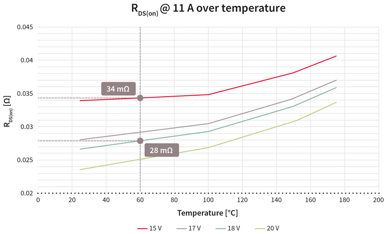
Figure 1: RDS(on) comparison for a CoolSiC device using various gate drive voltages at different temperatures
Switch mode power supplies (SMPS) have continued to improve in the overall efficiencies that are attainable when using classic silicon (Si) MOSFET technology. This has been achieved by pushing the boundaries with new silicon fabrication processes, design methodologies, and using these devices in innovative new topologies. Over the past few years, wide bandgap technologies have emerged, such as silicon carbide (SiC), that offer an array of exciting characteristics that enable engineers to achieve higher efficiencies but these must be weighed up against the price difference between the two technologies. With the introduction of 650 V SiC MOSFETs, to complement existing ranges of 1200 V devices, SiC has become more attractive for applications where, previously, it might have not been considered.
SMPSs are used in a wide variety of application spaces. Traditional general power supplies are the obvious solution, but others range from photovoltaic and wind power to motor drives and electric vehicle charging. At the higher voltages, above 1000 V, IGBTs have been the core technology of choice with SiC starting to encroach into certain spaces, specifically where high-frequency switching is desired and higher power density must be achieved. In the 650 V range SiC enables highly efficient topologies such as the continuous conduction mode (CCM) power factor correction (PFC). This is suitable for a wide variety of applications such as servers, telecoms, battery formation, and EV charging, just to name a few. These applications benefit from increased system efficiency, robustness and total cost of ownership (TCO).
Clarifying some of the benefits
One of the first requirements when considering the best time to make the change is looking at the target efficiency and power density of the application. Compared to Si MOSFETs, SiC provides a much more stable RDS(on) over its operational temperature range. Whereas Si MOSFETs are usually promoted with their maximum RDS(on) at 25°C, SiC MOSFETs highlight their typical value at 25°C together with a gate drive voltage (typically 18 V) and at a specific current (ID). A typical CoolMOS device can suffer an expected 1.67 times increase in RDS(on) between 25°C and 100°C, while a comparable CoolSiC device will undergo just a 1.13 times increase. This means an 84 mΩ CoolSiC MOSFET could have the same conduction losses as a 57 mΩ CoolMOS switch at the target operational temperature. With the higher operating temperature having a lower impact on performance, higher densities of design become possible while also simplifying cooling approaches in some cases.
A move to SiC can also see the use of the same drivers used for traditional Si devices that generate a gate drive voltage of up to 15 V. However, the RDS(on) is also impacted by the gate drive voltage used, so it is worthwhile considering making some small changes here. CoolSiC MOSFETs benefit from the use of a 0 V to 18 V gate drive voltage, and this can reduce the RDS(on) by 18% compared to using 15 V (at 60°C) (figure 1).
Care should also be taken to avoid the application of negative voltages to the gate of a SiC MOSFET, as this can cause the gate threshold voltage, VGS(th), to drift. Studies have shown that this can result in the RDS(on) increasing by a small amount over longer periods of operation. The VGS(off) level can go negative due to the high di/dt that results from the voltage drop over the source inductance in the gate-drive loop. It also occurs at very high dv/dts caused by the gate-drain capacitance of a second switch in half-bridge configurations, an effect that is often the greater of the two challenges. Obviously reducing the dv/dt and di/dt would tackle this issue, but this would lead to reduced efficiencies.
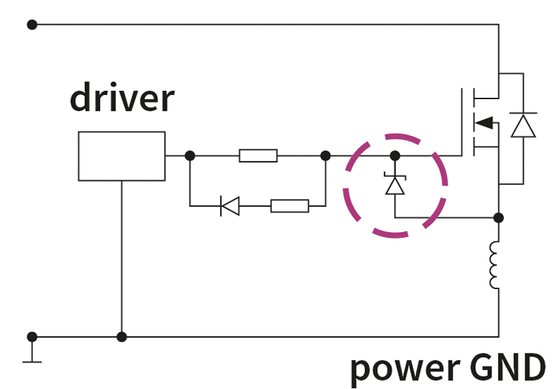
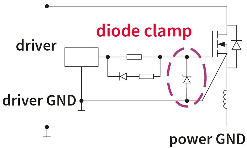
Instead, it is recommended to use a clamping diode between the gate and source of the switch that limits the negative voltage applied to the gate to above -2 V, leaving the device protected from VGS(th) drift. If desired, further approaches to reduce the effect of inductive-driven cases can be undertaken that are simple to implement. This requires that the driver ground and power ground are separated, thereby removing the source inductance from the gate drive loop. Using the Kelvin source, where available, can also provide a significant improvement in efficiency, especially at the highest current drain currents (figure 2).
Click image to enlarge
Click image to enlarge
Figure 2a and 2b: A diode clamp, separate power/drive circuits, and use of the Kelvin source all contribute to limited negative gate voltages
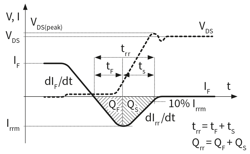
Impact of reverse recovery charge on topology choice
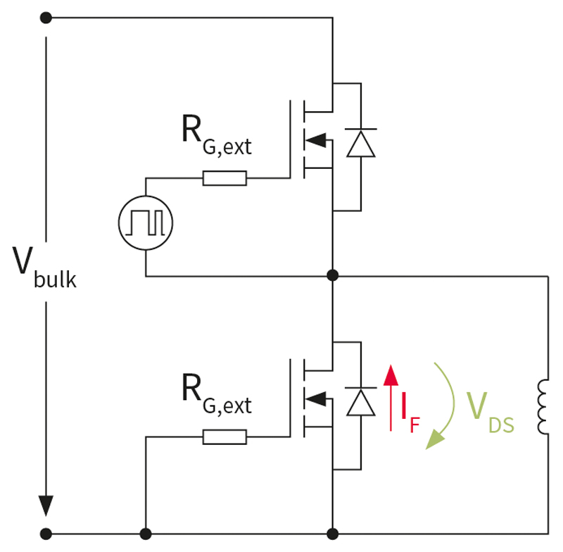
The reverse recovery charge (Qrr) is one of the most important parameters to be considered, especially for resonant topologies or designs that make use of continuous hard commutation on the conducting body diode. All MOSFETs have an inherent body diode in their design and Qrr represents the charge that needs to be removed from it after it ceases to conduct (figure 3). The semiconductor industry has done much to reduce this value with devices from the CoolMOS family being developed to integrate improved fast body diodes. While these changes led to a ten-fold reduction in Qrr over previous MOSFETs, CoolSiC switches provide a further ten-fold improvement over the latest fast diode CoolMOS devices.
Click image to enlarge
Click image to enlarge
Figure 3a and 3b: Qrr is the charge that needs to be removed from the body diode after conduction, highlighted by the area below the 0 A line
With the industry focusing on attaining 98% system efficiency at 50% load, pressure is placed on the power factor correction (PFC) stage to attain efficiencies of 99% or better. Without this, the likelihood of achieving the desired system efficiency is severely diminished. Thanks to the improvements in Qrr that CoolSiC switches provide, the use of hard switching topologies for the PFC becomes possible. Rather than using a triangular current mode (TCM) approach as would be recommended with CoolMOS, a continuous conduction mode (CCM) Totem Pole PFC can be implemented.
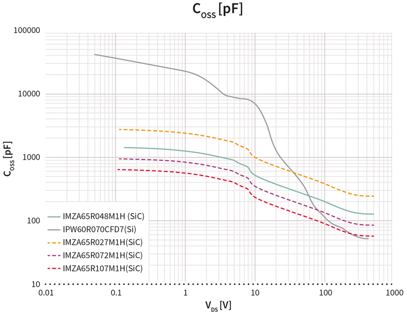
Output capacitance in SiC
Another important factor in MOSFETs of both technologies is the output capacitance COSS. The energy that builds up here, EOSS, has to be dissipated during non-zero-voltage turn-on. While a lower capacitance allows the use of higher switching speeds, it also results in drain-source (VDS) overshoot during turn-on. With CoolMOS switches, this has to be compensated for by using a resistor in the gate (RG) to slow down the switching speed. This also helps to achieve the required 80% de-rating on the drain-source. However, inserting RG has a down side in that it contributes to switching losses, specifically during turn-off as the current increases.
Click image to enlarge
Figure 4: Comparison of COSS for different VDS of CoolMOS and several CoolSiC devices
Although CoolSiC devices actually have a higher COSS than comparable CoolMOS devices at VDS values starting around 50 V - 60 V, they actually offer a much more linear relationship between COSS and VDS. This means that, in the same circuit, CoolSiC switches can be used with a reduced external RG resistor while still attaining the required 80% derating. This can be advantageous in some switching topologies, such as resonant LLC DC/DC converters (figure 5).
Click image to enlarge
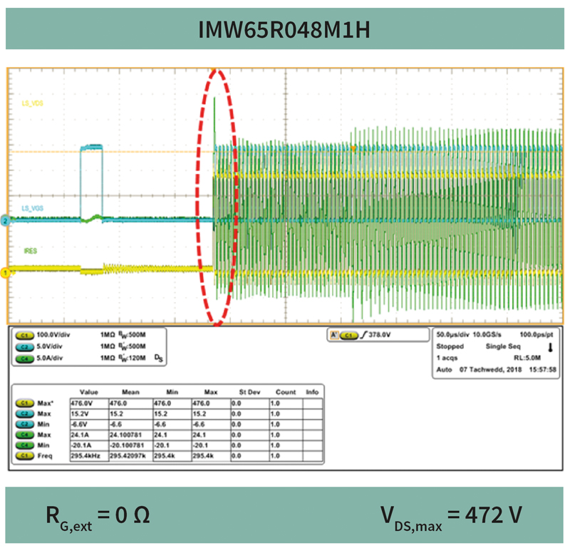
Click image to enlarge
Figure 5a and 5b: A resonant LLC at start-up achieves the 80% de-rating easily with a CoolSiC MOSFET without the need for an RG resistor
While SiC technology may seem to only offer advantages, this does not mean that Si MOSFETs can be simply replaced with SiC alternatives to attain better SMPS performance and efficiency. One important point to consider is the much higher forward voltage of the body diode, which is some four times higher than a comparable Si device. Simply swapping out Si for SiC will inevitably lead to body diode conduction losses that are around four times higher. This would mean missing out on a potential efficiency improvement of 0.5% under light load conditions. In order to attain peak efficiency, it is essential that the design provides the boost through the channel and not the body diode. In practical terms, this means altering the dead time used, optimising it to so that the full advantages SiC MOSFETs offer can be attained.
Conclusion
As more SiC MOSFET solutions in the 650 V class enter the market, the technology starts to become more attractive for wider range of applications. These include systems looking to attain ≥ 97% efficiency, converters where hard commutation is present or can occur, and high-power applications. It should, however, be understood that the characteristics of SiC and Si MOSFETs are quite different. Although much of existing SMPS designs can be retained, modification of specific aspects of the circuit, such as the gate drive voltage and dead-time implementation, will ensure that the full advantages of SiC are delivered in the final product.