GaN E-HEMTs are overtaking silicon (Si) MOSFET-based designs because of their superior performance
For the better part of this decade, power electronics technologists have been enabling new topologies with GaN (gallium nitride) transistors. Similarly, system innovators have been creating new levels of performance in electric and autonomous vehicles, industrial machines, televisions, laptop adapters, data centers, and automation for factory and homes with GaN. Until recently, these examples of GaN enhancement mode high electron mobility transistors (E-HEMTs) based designs have been happening in advanced research and pre-production programs. However, GaN-based power electronics have broken through the barriers of adoption and mass production is now happening.
GaN E-HEMTs are systemically overtaking silicon (Si) MOSFET based designs because of their superior performance. GaN E-HEMTs with their lower conduction and switching losses result in higher efficiency, less heat, smaller heatsinks, and higher power density. Along with the lower losses come higher switching frequencies with clean switching edges. This is creating smaller, lighter, and more efficient power converters in key applications. This is accomplished by smaller, lower weight, and less expensive magnetics and capacitors in the power circuit. The specific characteristics and construction of GaN transistors result in no reverse recovery current. This is a major differentiator to Si MOSFETs that allows for the highly efficient, low EMI bridgeless totem pole power factor correction (BTP PFC) topology. The increased switching speed and transitions also mean that traditional semiconductor packaging is not sufficient to take full advantage of GaN technology at higher power levels (> 500 W). GaN Systems implemented GaNPX® packaging technology that increases current density, improves thermal performance, and greatly reduces package inductance to fully exploit the advantage of GaN. The GaNPX® technology eliminates wire bonds, and hence the failure modes associated with them, and increases reliability of the transistor and power electronics system.
Figures 1 (a) and 1 (b)show simplified circuit of GaN Systems’ E-HEMTs and its gate drive circuit. GaN E-HEMTs are easy to drive with minimal gate drive components. The drive circuit is similar to that of Si MOSFET but achieve much better performance due to state-of-the-art figure of merit (FOM), see table 1. Another key advantage of GaN E-HEMTs is easy paralleling capability. To achieve higher output power, e.g. 22 kW on board charger, paralleling discrete power transistors is required. The characteristics of GaN Systems’ E-HEMTs are inherently fit for paralleling. The factors for paralleling are temperature coefficient of RDS(on), threshold voltage VGS(th), temperature coefficient of trans-conductance gm, and packaging. In parallel applications, the junction temperature of low RDS(on) GaN E-HEMTs increase to balance current sharing during the on-state because of positive temperature coefficient of RDS(on). The trans-conductance gm decreases with higher temperature and this characteristic together with stable gate threshold over temperature range help with dynamic current sharing and self-balancing. GaNPX®package has ultra low source inductance which will improve the paralleling performance and stability. In addition, GaN Systems provides dual gate pads feature which enables easier symmetric PCB layout in parallel application.
GaN Systems E-HEMTs provide better performance compared to Gate Injection Transistor (GIT) technology, a different gate technology. GaN E-HEMTs can easily adjust the slew rate by changing gate resistors Rgon/Rgoff. In contrast GIT GaN requires special drive design, with additional components like speed-up capacitor Cs and steady-state resistor Rig (see Fig. 2), adding design complexity to ensure not to exceed the rating of gate current.
 Simplified circuit of GaN E-HEMTs.JPG)
Click image to enlarge
Figure 1(a). Simplified circuit of GaN E-HEMTs
 GaN E-HEMTs gate drive circuit.JPG)
Click image to enlarge
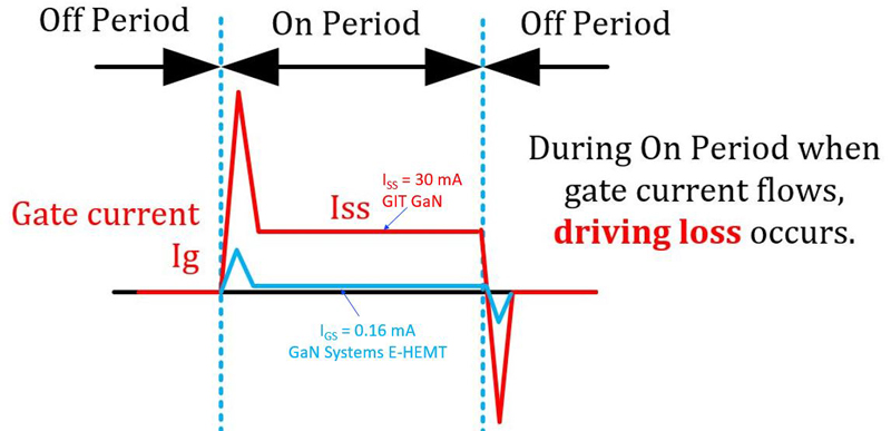
GIT GaN requires steady-state gate current of several mA to keep the intrinsic gate diode fully biased in the forward direction and thus maintain full rated drain current (see Fig. 2). This causes larger driving loss than GaN E-HEMTs. During the on-time, the additional steady-state charge, Qss, the integral of the steady-state gate current, is expressed in simplified form as Qss = Iss x tss. Fig. 3 shows gate driving current of GIT GaN, from off to on periods, during which driving loss occurs. GaN Systems E-HEMTs have a low gate leakage, IGSS, which results in low driving loss.

Click image to enlarge
Figure 2. GIT GaN power transistor’s drive circuit
Click image to enlarge
Figure 3. GIT GaN power transistor’s gate drive current
Table 1. Comparing Electrical Characteristics of GaN E-HEMTs and GIT GaN power transistor

Click image to enlarge
Table 1 shows the electrical characteristics of the GaN E-HEMT (650 V, 30 A) from GaN Systems and a GIT GaN power transistor (600 V, 31 A). These characteristics have a major influence on the fundamental performance of the devices. GaN E-HEMT provides smaller package size resulting in smaller footprint, higher maximum drain-to-source voltage, and better figure of merit. Fig. 4 shows the gate drive loss comparison using the transistors in Table 1. The steady-state gate current, 30 mA, is from the GIT GaN datasheet, when VGS is 3.5 V at 25 °C. This gate current will increase with temperature. Comparing the two technologies at 500 kHz switching frequency, the gate drive loss of GaN E-HEMT is 0.0174 W, while that of GIT GaN is 0.19 W. The GaN Systems E-HEMT loss is 11X lower than the GIT GaN, which is important for efficiency in 500 W and below applications.

Click image to enlarge
Figure 4. Gate Drive Loss Comparison
Switching and conduction losses in GaN E-HEMTs are calculated and measured in the same way for GaN E-HEMTs as they are for silicon MOSFETs or any other switching power transistor, however the results for GaN are much better. Switching losses occur during the transition from the transistor being off (gate voltage = 0 V, drain-to source = VBUS) to on (gate voltage rises to 6 V, drain-to-source voltage drops to approximately 0 V) and then again when the transistor transitions from on (gate voltage is at 6 V, drain-to-source voltage approximately at 0 V) to off (gate voltage drops to 0 V drain-to-source voltage rises to VBUS). Conduction losses occur while the transistor is on (after the turn on transition and before the turn off transition), that is, while conducting drain to source current. The difference in losses between GaN E-HEMTs and Si MOSFETs is clearly apparent when looking at Fig. 5, a representation of a turn-on and turn-off cycle of a GaN E-HEMT. Also represented in Fig. 5 is a turn-on transition of a switching Si MOSFET. The turn on time for a GaN E-HEMT (650 V, 30 A) is less than 5 ns. This turn on time is typically 10 times less than a comparable (650 V, 30 A) Si MOSFET which lowers the associated turn-on losses are lower by the same order. Similarly, the turn-off times for GaN E-HEMTs are 10 to 20 times lower that the turn off time in comparable MOSFETs.
Conduction losses are calculated by multiplying the square of the drain-to-source current by the RDS(on) of the transistor. Silicon MOSFETs have traditionally been characterized by a static RDS(on) test which is performed by applying a current from drain-to-source while the gate voltage is fully enhanced. The RDS(on) of Si MOSFETs during their intended operation in switching power electronics is accurately characterized by the static RDS(on) test. This can be seen in Fig. 5 by the relatively flat voltage after the long turn on period of the MOSFET voltage waveform. GaN E-HEMTs, however, are slightly different. Due to the construction of GaN-on-Si transistors, trapped charge exists in a 2-dimensional electronic gas (2DEG) barrier. This trapped charge decreases during the on time of the GaN E-HEMT and is highest immediately after the turn on-period. The outcome is that the effective drain-to-source resistance is slightly higher at the beginning of a switching cycle and decreases to a steady state nominal value towards the end of the duty cycle. While a static RDS(on) measurement of a GaN E-HEMT gives valuable information about the transistor, it does not fully represent the effective RDS(on) of the device. The effective RDS(on) of GaN E-HEMT is represented by the static RDS(on) plus a small and variable dynamic element. The static RDS(on) element represents the bulk of the effective RDS(on) as in Si MOSFETs. The dynamic element of effective RDS(on) is dependent on several factors in a switching application, like VBUS, switching frequency, and duty cycle. Better methods of testing and characterising effective RDS(on) than are currently practiced are being developed by GaN E-HEMT industry leaders like GaN Systems.

Click image to enlarge
GaN E-HEMTs are now the transistor of choice for high performance power electronics because they allow the design and real production of significantly more compact and efficient power converter designs. This is enabled by GaN E-HEMTs low capacitance, low gate charge, low on-resistance, and high voltage capability. GaN Systems E-HEMTs extend the value of GaN by offering the lowest power and simplest gate requirements. Better characterization and understanding of the effective resistance of GaN E-HEMTs are reinforcing the benefits of GaN. GaN in power conversion is here to stay.
The authors wish to thank Dr. Roy Hou for his valuable contribution to this article.
GaN Systems, Inc.